The Top 10 PCB Routing Tips for the Beginner
There’s an old saying that goes something like this – PCB design is 90% placement and 10% routing. This is still true today, and the placement of your components will end up deciding how much time your routing will take, but that doesn’t mean that routing your PCB is any less important. It’s simply a matter of how much time you spend on each activity.
If this is your first time doing a PCB layout, then seeing a chaotic looking ratsnest might be a little intimidating. Use these top 10 PCB routing tips and also our top 10 component placement tips to make your first PCB layout a success.
Tip #1 – Don’t Rely On Your Autorouter
There’s a tool tucked into nearly every PCB design software out there called the autorouter, and as a beginner, your eyes might light up thinking this is an easy way to solve your routing problems. But wait! Autorouters, as good as they can be, are never a replacement for routing yourself, and should only be used for a few reasons, including:
- Precision. You can use the autorouter after you place all of your components to see what completion rating you get. If it’s below 85%, then this is an indication that you need to make some adjustments to your part placement.
- Bottlenecks. You can also use the autorouter to discover bottlenecks and other critical connection points that you might not have seen during your component placement process.
- Inspiration. Lastly, you can use the autorouter as a source of inspiration for how you might want to route some traces that you just can’t complete. A quick run through the autorouter might show you a new path that you hadn’t considered before.
Outside of these three reasons, we’d recommend not relying on your autorouting to complete all of the routing on your board layout. Why? It’s not always the most accurate, and if you’re a fan of symmetry, then your autorouter will most likely disappoint. And most importantly, you’re the master of your design, and you’ll be able to produce way better results by doing the routing process yourself. It’s a carefully crafted process that requires some love and attention to get the results you want.

Tip #2 – Understand Your Manufacturer’s Specifications
Before you start laying down a copper trace, first take the time to give your manufacturer a call or shoot them an email to see if they have any specific requirements on minimum trace widths, trace spacing, and the number of layers they can handle on a board (for the right price)
Why? By knowing this information up front, you can set your trace width and spacing values in your design rules and avoid having to re-route your entire board layout down the line. And by using trace widths and spacing that your manufacturer can produce, you’ll make everyone’s life easier when it comes time to make your board.
Tip #3 – Figure Out Your Trace Widths
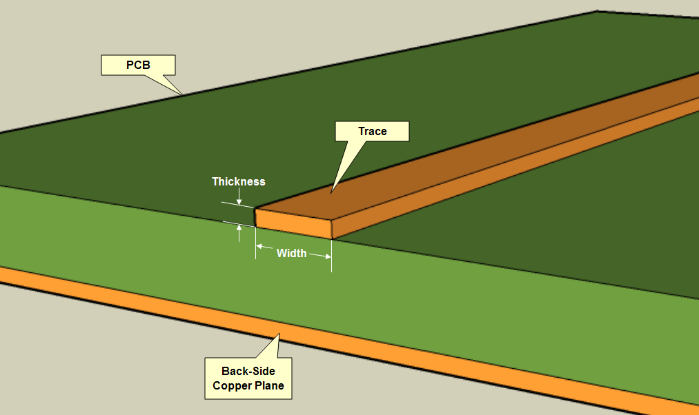
When you have electricity cruising through all of your copper traces, it’s going to produce some serious heat, and this is always a concern with electronics. Controlling the width of your traces is one of many ways to reduce how much heat builds up on your board, and the wider your traces, the less resistance that electricity will encounter when flowing through your circuit.
To determine the thickness of your traces, you can use a handy trace width calculator like this one from Advanced Circuits that will allow you to plug in your estimated current and thickness and get a trace width value in return for internal and external layers. A word of advice – if you have the opportunity to use larger trace widths than what your calculator shows, go for it! So long as you meet your manufacturer’s requirements then the larger your traces are, the less likely you are to get a board back with broken connections.

Tip #4 – Leave Enough Space Between Traces
It’s important to leave enough room between all of the traces and pads on your PCB layout. Why? If you pack things too close together, then you’ll run the risk of a short circuit developing when your board gets manufactured and traces unintentionally connect.
Remember, the PCB manufacturing process isn’t 100% precise, so you always need to leave some leeway in spacing between components pads and traces to stay safe. As a bare minimum, we recommend always leaving a gap of 0.007” to 0.010” between all adjacent pads and traces on your board.
Tip #5 – Make Your Job Easier with the Snap Grid
In Autodesk EAGLE you have complete control over your snap grid settings, which comes in handy during both your component placement and routing process. There’s no reason to not turn on your visible grid snap, and you’ll thank yourself later when you start to work with denser board layouts that need precise placement of traces and parts.
As a guiding rule, we recommend setting your snap grid spacing to 0.050” for your routing process. You can also set your alternative spacing to 0.025” when you need to design a tightly spaced connection between components. And of course, always have your visible grid set to On!
Tip #6 – Avoid Using 90 Degree Trace Angles
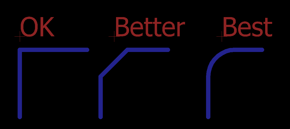
You’ll hear this time and time again if you talk to engineers and manufacturers, don’t use 90-degree trace angles. Why? When you have a bunch of traces that have a sharp, right angle turn on your board, the outside corner of that 90-degree angle has the likelihood of being etched narrower than your standard trace width. And at its worst, you might get a bunch of 90-degree traces back that aren’t fully etched, resulting in shorts.

As a solution to this problem, try to use 45-degree angle traces. This will produce some beautiful PCB layouts while also making your manufacturer’s life easier by being able to easily etch away all of the copper on your board.
Tip #7 – Leave Room Between Traces and Mounting Holes
In your component placement process, you likely placed all of your mounting holes first, but did you toss them down leaving enough room between other components and all of the traces that will connect them together? If you didn’t, you might run the risk of creating a shock hazard on your board, and relying on the soldermask as your one and the only insulator isn’t a guarantee of safety. So when working with mounting holes, always remember to leave a ring of space beyond the physical dimensions of the mounting hole to protect it from other components and traces nearby.

Tip #8 – Always Create a Ground Plane
Having a common ground on your PCB is imperative as it gives all of your traces the same reference point for measuring voltage. This comes in handy if you’re working with an analog circuit as your first design. If you use traces to route to ground instead of using a ground plane, you’ll find yourself with a multitude of different ground connections on your board, all with their own resistance values and voltage drops, which can be a nightmare.
To avoid all of this nonsense, we always recommend creating a dedicated ground plane on your PCB layout. This can be a large copper area on a single layer board or even an entire layer dedicated as a ground plane on multilayer boards. And once your ground plane has been added, it’s simply a matter of connecting all of your components that need to go to ground with vias.

Tip #9 – Make Your Power and Ground Traces Wider
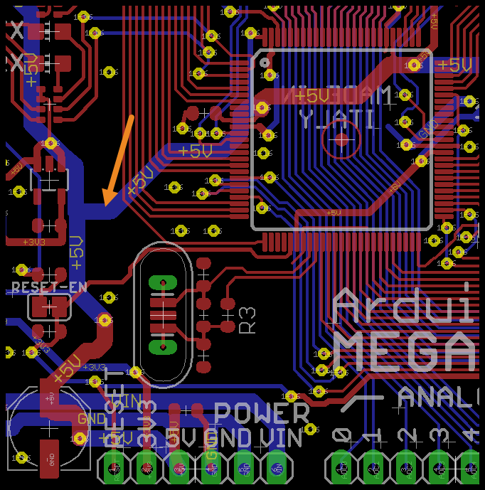
Not all of the traces on your PCB layout are created equal, and you’ll want to make sure that you increase the width of your traces that are going to serve as your power and ground paths. Why? Both power and ground traces will have more current flowing through them, and if you don’t make them wider than average, you’ll get a ton of heat trying to flow through those skinny spaces, which can end up burning wires and ruining your board.

By making your power and ground traces as thick as possible, you’ll also be able to quickly recognize them if you ever need to review and make adjustments to your design in the future.
Tip #10 – Use Vias to Remove Heat
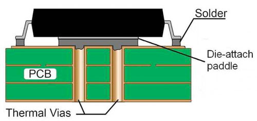
Our last and final tip has to do with vias, which seem to be the jack of all trades on a PCB layout. Not only are vias ideal for providing electrical connectivity between layers, but they’re also the perfect tool to use when you need to move heat from one side of your board.
This comes in handy if you ever need to channel heat away from one of your super powered components, like an integrated circuit (IC). By placing multiple vias below the die of an IC, you’ll be able to lower the operating temperature of a component, which will, in turn, make your design all that more reliable in the long run.

Route On!
Even the best component placement can become unraveled if you don’t take the time to think about how you plan to route all of your traces. Did you remember to give all of your integrated circuits enough room to have all of their pins connected? And do those mounting holes have enough space? Considering all of these questions and more will help to turn your first PCB design process into a success. Just like the component placement process, you’ll likely find that PCB routing is just as creative and artistic, and there’s nothing like seeing a gorgeous PCB layout with 45-degree traces dancing all over the place. But remember, that sought-after symmetry will come at a cost to your time, but it’s worth it. So remember to avoid that itch of using the autorouter and route your board manually!
Ready to start your first PCB design project? Try Autodesk EAGLE for free today!