The Top 10 Soldering Issues That Can Ruin Your PCB Design
If you’re making production level PCBs, then chances are you won’t be manually soldering components by hand. At this point, it’s all about relying on your manufacturer to both fabricate your bare board and assemble all of your parts for you. While the soldering process with a manufacturer still relies on the same principles you used on your prototypes back in your lab, there’s now some heavy-hitting machinery at play to get the job done. But just because there’s machinery involved doesn’t mean that this process is any less error prone than doing it by hand. Soldering at the manufacturing level is still very much a precise science that needs to be carefully controlled. Otherwise, you’ll wind up with one of these 10 soldering issues.
Wave Soldering 101
If this is your first PCB design that you’re relying on a manufacturer to fabricate and assemble for you, then wave soldering might be a new term. This is the process of sending your PCB through a giant oven where all of your components get attached to your board in a matter of seconds. As you can imagine, this process is way more efficient than having to manually solder components by hand, and the machinery involved can handle both through-hole and surface mount components at the same time.
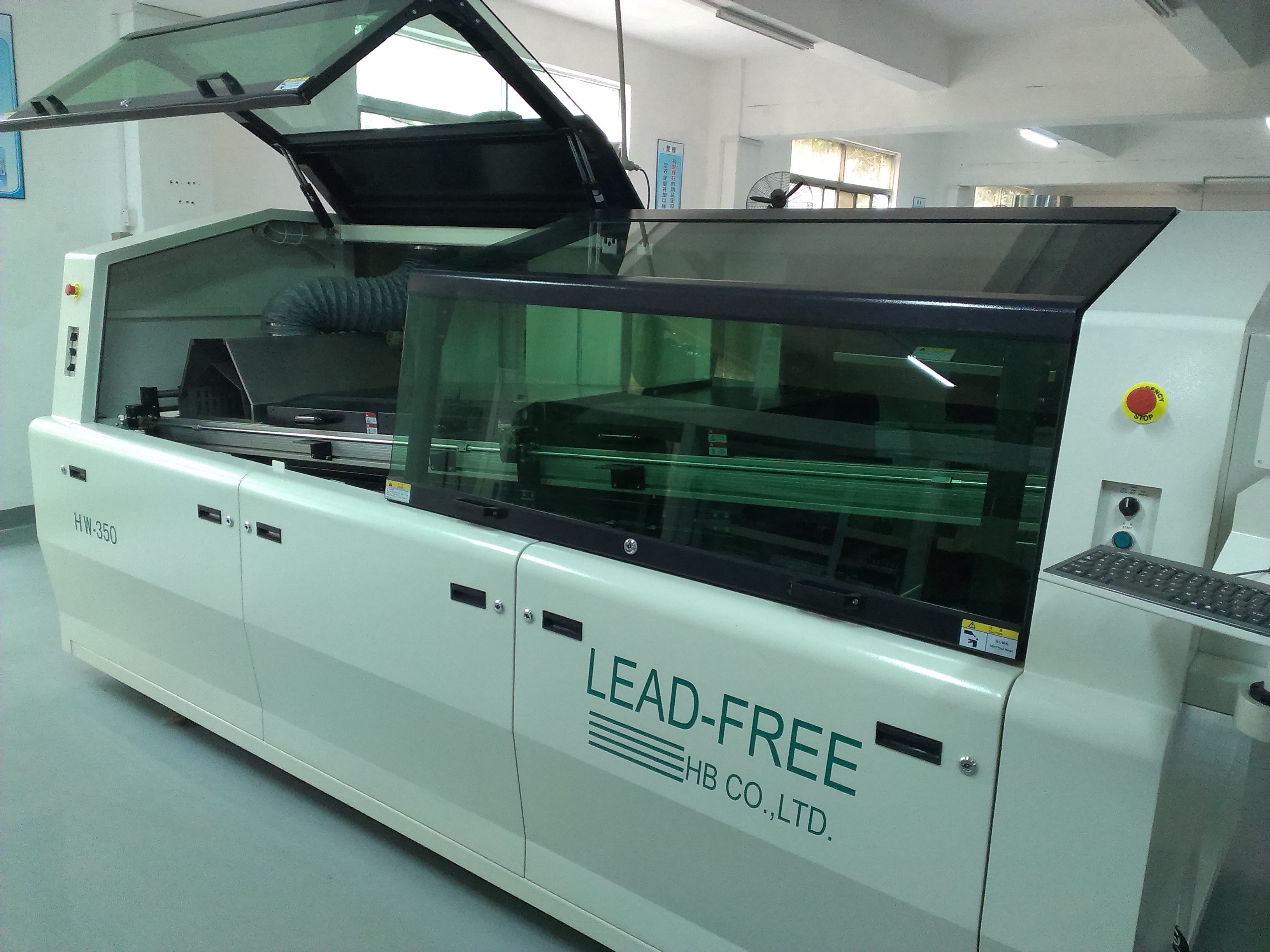
The wave soldering process uses a wave soldering machine as shown in the image. This machine is a self-contained oven that takes a bare board with placed components on one end and provides a fully soldered board on the other end. In between this start and end point are several processes, including:
- Flux Application. Your board is first placed on a conveyor belt at the onset of the wave soldering machine, and a flux layer is applied. This layer cleans all of your components and ensures that solder can attach properly to the pins and pads on your components.
- Preheating. After passing through a flux application, your board then rests on a preheating pad. This process heats your board just enough to prevent any thermal shock before it heads into the soldering wave.
- Soldering Wave. This final stage is where your board passes over a liquid soldering wave. The bottom layer of your PCB will make contact with a liquid wave of solder, forming a connection between each component and their associated hole or pad.

As you can see, this self-contained wave soldering process has many opportunities for mistakes from flux application to the final wave soldering process. We’ll be exploring below how these processes can interact together with your physical circuit board to cause some unintended issues.
Note: If your board ends up having soldering issues, it’s not always your fault. Yes, there are specific decisions that you need to make during your design process that will affect the manufacturability of your board, like component spacing, orientation, etc…But outside of that, many issues arise during the wave soldering process because of problems on your manufacturer’s end that need to be corrected.
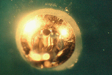
Don’t immediately place the blame on yourself if your board gets messed up due to soldering issues. The post-manufacturing analysis process will reveal the root cause, whether that’s a defect in your design or a problem with your manufacturer’s process or materials. When you or your manufacturer are looking for defects, it’s always good to have an ideal image in your head of a healthy solder joint. Check it out below.

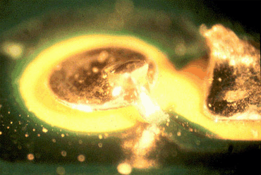
#1 – Solder Bridging
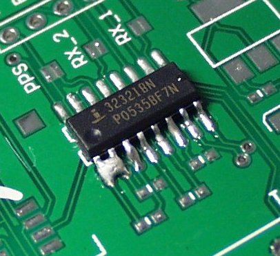
Solder bridging occurs when two solder joints connect, forming an unintended connection that can lead to short circuits on your board. As you can see in the image above, the first two pins on this IC have bridged together. Not good.
Some causes for solder bridging can include:
- Designing a PCB with poor weight distribution with large components all on one side.
- Not leaving enough space between your pads and your solder mask layer.
- Not orientation components of the same type in the same direction.
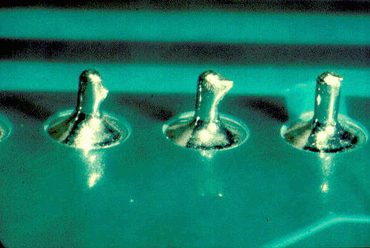
#2 – Lifted Components (Tombstone)
Having a tombstone component on your board means that it raised off the base of your PCB during the wave soldering process. This ends up looking like a tombstone.
Causes for this type of issue can include:
- Having an incorrect lead length that lifts when entering a solder bath.
- Wave soldering a flexible PCB that bends while the components stay flat.
- Using components that have varied thermal or lead solderability requirements.
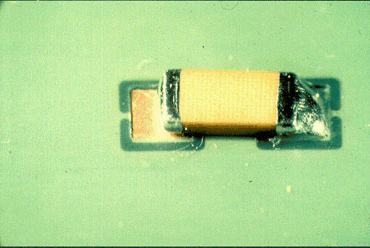
#3 – Excessive Solder

If your board passes through a wave soldering machine and takes too much solder with it, you’ll get an excess buildup. And while this excess solder might still be forming an electrical connection, it becomes hard to tell what’s going on inside that rounded mass.
Causes of excessive solder can include:
- Not orientation components of the same type in the same direction.
- Using an incorrect lead length to pad ratio during your design process.
- On the manufacturer’s end, the conveyor belt might also be running too fast.
#4 – Solder Balling
Solder balling occurs when a small bit of soldier attaches itself to the surface of your PCB during the wave soldering process.
Causes of solder balling can include:
- The solder temperature being too high in the wave soldering machine.
- Solder falling back into the solder wave during separation and splashing back onto your board.
- The gasses released when the flux is heated causing solder liquid to spit back up onto your board.
#5 – Solder De-Wetting/Non-Wetting

When your solid is “wet,” this is a good thing. It means that your solder has reached an ideal fluid state and will be able to properly attach to a component lead or pad. There can be two issues with this wetting process. The first is de-wetting, where molten solder covers a lead or pad and then retreats, leaving behind an oddly shaped mound of solder. There’s also non-wetting, where solder only partially attaches to a surface, leaving exposed copper behind.
Causes of both of these wetting issues can include:
- A manufacturer’s component inventory not being properly rotated. Many parts only have a solderable shelf life of about a year.
- The flux being used by your manufacturer might be past its prime and needs to be changed after forty hours of use.
- The plating used on brass component pins might not have been properly plated with copper.
#6 – Lifted Pads
If a component is mistakenly soldered and needs to be removed, this can lead to the pad of said component lifting from your PCB.
Causes for a lifted pad can include:
- Overworking the pad joint too much where the layer between the copper and your board is ruined.
- Boards designed with thin layers of copper being more susceptible to this problem.
- Your board might not have received an even layer of copper plating for through-hole component leads.
#7 – Pin Holes & Blow Holes
Pin holes and blow holes are easy to identify, just look for the hole in a solder joint. This hole might extend all the way from the layer you’re observing to internal layers, or even the bottom of your board, causing connectivity issues.
Causes for these holes can include:
- Excess moisture building up in your board that will try to escape through thin copper plating.
- Not orientating components of a similar type in the same direction, which can lead to a poor copper plating process.
- During your design process having a lead-to-hole ratio that is either too small or too large.
#8 – Solder Skips
As the name suggests, solder skips can occur when solder skips over a surface mount pad, leaving an unconnected area or pad.
Causes for solder skips can include:
- Your manufacturer using an incorrect wave height between your board and soldering wave.
- The gassing of flux beneath your board causing the solder to not properly adhere to a joint.
- During your design process, placing down uneven pad sizes for an SMD component.
#9 – Solder Flags
While solder flags themselves will still leave the proper connection on your board, they are an indicator of poor flux application and solder drainage issues and may “flag” solder issues in other places on your board.
Causes for these protrusions from a solder joint can include:
- The solder draining slowly from a wave soldering machine, leading to an excessive height of solder.
- An inconsistent application of flux, which can be identified if you see whisker-like trails of solder on your board.
- If your component supplier cuts the leads on your parts and stores them for long periods of time, this can cause oxidation and solder will struggle to attach.
#10 – Solder Discoloration

This last soldering issue is purely a cosmetic one, but your manufacturer should take the time to find out the root cause. Finding discolored mask can be identified on the solder resist, your PCB, and even the conveyor belt in the wave soldering machine.
Causes of solder mask can include:
- Your manufacturer using different flux materials or higher temperatures between wave soldering runs of the same board.
- Your manufacturer changing the soldermask type or thickness halfway through a soldering cycle.
- Your manufacturer mixing batches of circuit boards during the same wave soldering process.
Ride the Wave
There you have it, the top 10 soldering issues that can ruin an otherwise great PCB design. Again, keep in mind that all of the issues we described above are not necessarily your fault if they occur. If you happen to be following a Design for Manufacturing (DFM) set of best practices, then the issue most likely falls on your manufacturer. Of course, all of these soldering issues should be identified by your manufacturer during the inspection phase. If a problem is found, it’s then a process of finding the root cause, whether that’s an issue with the wave soldering process or a problem with your design. To keep yourself ahead of the game and avoid soldering issues, always keep a DFM checklist on hand to make sure you’re meeting your manufacturer’s best practices. That way you can get a good board back right the first time, every time.
Ready to design and manufacture your first professional PCB? Try Autodesk EAGLE for free today.