The Top 10 Tips to Draw Your Next Schematic Design Like a Pro
Ready for that next great idea for a PCB project? It’s all starts with your schematic design. Unlike a PCB layout, which is all about the physical placement of parts and copper, a schematic is more theoretical, describing how components are electrically connected. And while you won’t necessarily know how parts physically connect when drawing a schematic, you will know exactly how a signal will move through your circuit. Sounds easy enough, right? Not so fast.
In the world of electronics design, there are good schematics, and then there are bad schematics. The difference ultimately comes down to a simple question – is someone going to be able to understand and troubleshoot your circuit based on your schematic immediately, or will reading your schematic just lead to more confusion? If you’ve been designing bad schematics in the past, or you just don’t know the best practices, worry not. Here we’ve got our top 10 tips that will show you how to draw your next schematic design like a pro!
Pro Tip #1 – Clearly Show How Your Wires Connect
You’ll be relying on wires to define connections between symbols on your schematic drawing. In Autodesk EAGLE you’ll see these referred to as nets. Regardless of what you call them, there are several guidelines to keep in mind.
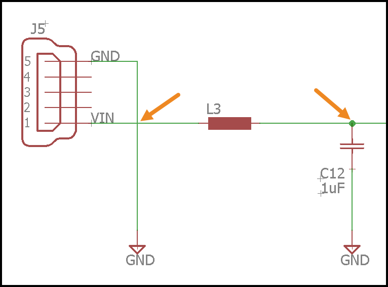
First, whenever you have two wires that form a junction and share an electrical connection, that intersection needs to have a junction dot. This is standard practice in every schematic design, and some tools like Autodesk EAGLE will add the junction dot for you. However, if you have a pair of intersecting wires that are not sharing an electrical connection and are just overlapping, then you will not need a dot. This lack of a junction dot will signify that the wires are only crossing.
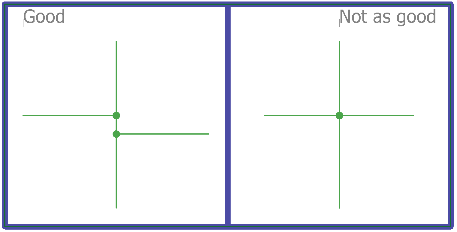
When adding junctions for intersecting wires, it’s also recommended to avoid a 4-way intersection as this will likely add to the confusion when reading your circuit. Instead, opt for a set of shared intersections as shown in the image below where each junction has its own unique connection. This makes it much easier to understand exactly the proper connections and avoid misinterpretation.
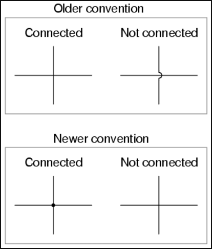
Last, you might have seen some schematics in the past with a curve on the part of a wire where it intersects with another wire. This was an old standard to signify that two wires were overlapping with no shared connection, but this is now an obsolete practice, so it is not recommended.
Pro Tip #2 – Complete Net Connections When It Makes Sense
The entire goal with a schematic is to make your circuitry as easy as possible to understand when you read it in the future or hand it off to another engineer. To aid with this process of readability, it’s necessary to minimize any unnecessary net connections when they aren’t needed.
You’ll commonly see this happening when you draw an integrated circuit (IC) symbol on a schematic. Rather than drawing dozens of nets all over the place, engineers will typically just signify a net name for a specific pin, which is associated with a pin on another device without the two needing to be connected. Doing this enhances the readability of a schematic without adding any unnecessary clutter.
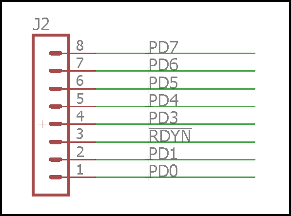
When in doubt, ask yourself as you are placing a net if it will help to enhance the readability of your schematic, or will it just add clutter? And on that same note, we also recommend keeping your net names as short as possible and in all caps. It’s much simpler and efficient to name a net as “CLK” than “10 MHz clock to PIC.”
Pro Tip #3 – Always Use the Same Symbol for the Same Device
If this is your first schematic drawing, then you might be surprised to know that there are several different ways you can draw schematic symbols. This all depends on what side of the world you’re living in, and what standard you plan to follow.
To keep things organized and consistent on your schematic, always use the same symbol to represent the same device. For example, placing an IEEE resistor on your schematic and a European IEC resistor will just lead to confusion.

Before drawing your schematic, take the time to review all of the known electrical symbols and use them consistently in every one of your projects. Here’s a great electrical symbol reference list that shows the most common types.
Pro Tip #4 – Make Sure Every Part Has a Unique Designator
This is another tip to enhance the consistency and readability of your schematic. Every symbol on your circuit needs to have its own unique designator so that every part is easily identifiable. For example, every resistor should follow a consistent naming sequence of R1, R2, R3, etc.
If you’re using parts form an existing Autodesk EAGLE library like those from Sparkfun or Adafruit, then these designators will already be set for you. But if you plan to make your own symbols then you’ll need to add the proper designator. Check out the list of designators below for reference in your future projects:
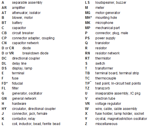
In this same line of thinking, if you are planning to use components with particular performance requirements, then also consider adding a label to the symbol. For example, you might need to add labels for parts that have specific trace width requirements, special shielding needs, or impedances.
Pro Tip #5 – Keep Your Text Placement Consistent
Building on Tip 4, there’s nothing more painful than trying to read a schematic that has symbol names, values, and labels in a mix of horizontal and vertical orientations. Just take a look at the schematic below, doesn’t that just make your head spin?

When placing symbols on your schematic, take the time to properly orient all names and values in the same direction, regardless of the placement the your component. This will make your schematic much easier to read and reference by your fellow engineers.
In Autodesk EAGLE this process is easy. Simply use the Smash ![]() tool on the left-hand side of your interface to separate the name and value from a symbol. From there you can rotate and orient symbol names and values.
tool on the left-hand side of your interface to separate the name and value from a symbol. From there you can rotate and orient symbol names and values.
Pro Tip #6 – Keep Your Schematic Arranged Logically
When drawing your schematic, it’s important to keep in mind how your circuit will logically flow. For most electrical schematics, with some minor exceptions, signal inputs will always come from the left and signal outputs will always go to the right. Power will start from the top and ground, or negative voltages will go to the bottom.
When drawing your schematic make sure that the placement of your symbols and the connection of your nets always follow this logical flow. This will make it a whole lot easier to reference your schematic in the future, and will also make it simple for another engineer to read.
Pro Tip #7 – Separate Your Schematic Into Logical Blocks
If you’re designing a complex circuit with multiple functions that can be logically separated, then do so. This makes it much easier to review and troubleshoot your circuit when major functional areas are clearly defined on their own separate sheet.
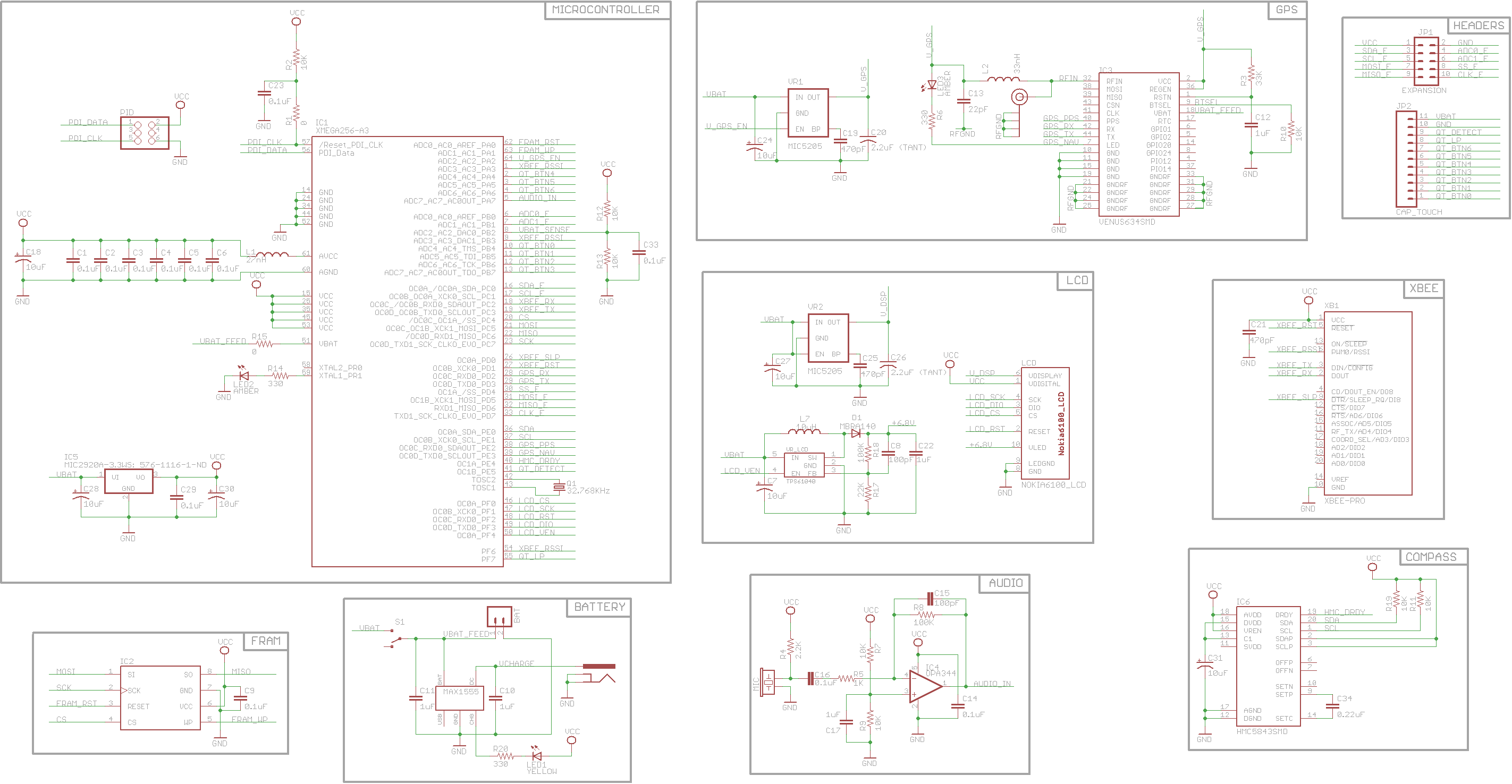
If your schematic isn’t large enough to require separate sheets for each functional block then at least consider adding frames around each section with a label in each. Also don’t be afraid to leave blank space on your schematic sheet. The goal isn’t to fill every inch of your schematic, but rather to keep your circuitry logically separated and organized for easy readability.
Pro Tip #8 – Design Your Schematic for Easy Printability
We recommend always drawing schematics that can be easily printed and reviewed on a standard sheet of paper. In the U.S. this is going to be 8.5” x 11”, and in Europe, you’ll find A4 sizing used, which measures in at 210mm x 297mm.
Why limit your schematics to this size? Simply because the days of engineers having giant drafting tables are gone. Most people only have access to printers with standard page sizes, and it’s just easier to print out a single page that can fit alongside your monitor and keyboard.
Because of this size restriction, we also recommend using multiple schematic sheets if needed to keep your schematic sections easily viewable without having to pan. Even if your schematic isn’t printed out, it’s just easier to page between multiple sheets in a PDF with their own functional schematic blocks than it is to have to pan around one giant sheet manually.
Pro Tip #9 – Place Decoupling Caps Next to Their Device
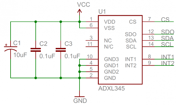
If there’s one exception to the rule that schematics are purely made for electrical connectivity and not about placement, then it’s for decoupling capacitors. These components are crucial when you need to smooth out a signal from a supply for those sensitive components like integrated circuits. When placing decoupling caps on a schematic, be sure to orient them in proximity to the component that they’ll be placed next to on a physical PCB layout. This will help another engineer to understand the intent of a group of capacitors quickly.
Pro Tip #10 – Remember Your Title Block
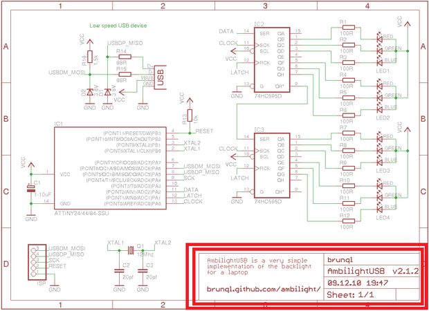
Last but not least, remember to always include a title block on each page of your schematic! This is a simple organizational tool that can help to keep track of multiple schematic sheets, know who designed them, and know what version of the design you’re viewing. When you add your title block, place it on the bottom right corner of your sheet(s) and include the following information:
- The name of the circuit, your name, and the date of creation
- The schematic sheet number if you have more than 1 page
- Also, consider adding a revision number to make it easy to differentiate versions
Design Like a Pro
There they are, the top 10 tips that can help you to draw your next schematic design like a pro! When it comes to schematics, your goal is always one focused on clarity. Is your schematic easy enough to understand at a glance by another engineer? And more importantly, will you be able to read and interpret what you’ve drawn if you pick your schematic up again a year from now? Schematics form the foundation to every electronics design, and it just makes sense to take the time to communicate information as efficiently as possible clearly. This will help if you need to pass on your schematic to another engineer for the PCB layout process, and will also help with troubleshooting your circuit in post-production. So what are you waiting for? Get out there and start drawing schematics like a pro! Your fellow engineers will appreciate you.
Ready to draw your next schematic with our top 10 tips? Try Autodesk EAGLE for free today!