Learn how to make your first high-speed PCB design a success by minimizing crosstalk, EMI, and more.

It wasn’t that long ago when the word “high speed” didn’t exist in the vocabulary of PCB designers. But these days, it seems to be just the opposite. Back then, the concern was all about putting the puzzle pieces together and strategizing your way through a physical board layout. But with high-speed PCB design? Now there are a bunch of invisible forces to worry about. Things like electromagnetic interference (EMI), crosstalk, signal reflection, and the list goes on. Here are some practical tips to make your first high-speed design process a success.
More data, more EMI
In 2005, 3 Gbps was considered the typical high-speed data rate, but today engineers deal with 10 Gbps and even 25. Not only are they dealing with that rate, but there is a constant push to get faster clock rates. Devices are getting smaller than ever to meet growing consumer demand. If you’re designing today, you most likely already incorporate some aspect of high-speed design. There’s DDR, PCI Express, USB, SATA, etc.
At the heart of high speed, PCB design is an issue of interference. The faster your data rates are, the more issues you have trying with to protect the integrity of your signals. Most of these problems stem from electromagnetic radiation. This radiation is relatively harmless in small amounts when it makes contact with a circuit. But when it starts to interfere with the operation of your electronic device as a whole, then radiation becomes interference. And Electromagnetic Interference (EMI) becomes a whole new world of issues! If you’ve ever heard or encountered issues related to noise, then you know exactly what we’re talking about.

So you might be wondering, how in the world do you ever know if you’re working on a high-speed PCB design project without discovering it through EMI issues? There are several schools of thought here, and we’ll break down the top 3:
- Frequency. The first thought is that high-speed design is categorized based on the frequency of a PCB and its ability to affect circuit performance. For some, this means anything above 50 MHz. Others categorize it into several buckets for low speed (<25 MHZ), moderate speed (25-100 MHz), high speed (100-1000 MHz), and anything above that is an ultra-high speed, reserved for RF designers.
- Traces. There’s also the school of thought that you can use the physical dimensions of your trace to determine if you’re working with a high-speed device. This guideline states that once a trace is more than ⅓ the rise time of your device’s switching speed, then you’ve got high speed.
- Separation. The last perspective takes a general approach, looking at your circuit design as a whole and asking the following question – does your system physically work together uniformly? Or do you have a bunch of subcircuits that are all organized into one larger circuit, with everything working together separately? The latter puts you into the realm of high-speed design.
Got your upcoming project classified as high speed? Great. That’s all the background noise you need to worry about. Let’s dive into our top 10 tips for a successful design process.
1. Always start your high-speed PCB design process with a plan
We’re starting with the most obvious tip, but for a good reason. Without a plan and a strategy for your high-speed PCB design project, you’ll likely encounter setbacks, respins, and unexpected issues. So before ever laying down a symbol or connecting a net, you need a checklist in hand for what lies ahead. Here are a few questions to ask yourself:
- System organization – Do I have a visual diagram that will help me to see how all of my sub-circuits interconnect and a well-established return current?
- Signal speed – Do I know the highest frequency and fastest rise time of each of my signals?
- Power supply – Have I documented every one of my voltage and power requirements for all of my IC? Will I need to split any power planes?
- Sensitive signals – Do I have a plan to meet my requirements for differential signals, controlled impedance, and trace length or propagation?
These are not the only questions to keep in mind during the planning stage, but they’ll get you started. You’ll also likely need to work with your manufacturer to understand their minimum tolerance requirements. And you’ll need to consider developing a strategy to reduce the level of noise on your high-speed signals with a variety of routing methods, including microstrip or stripline traces.

2. Document every detail of your board stack-up for manufacturing
To build off of the planning stage in Tip 1, it’s now time to define and document your layer stack-up requirements thoroughly. This is a perfect time to get together with your manufacturer to determine what materials of your board and what specific constraints you need to input into your design rules. As far as materials go, you’ll likely be working with one of these:
- FR-4. This is a great material when you’re working with clock speeds of < 5Gbps and is classified as a low-speed material. FR-4 has a decent ability to control impedance and is also known for its low cost.
- Nelco, SI, or Megtron. In the realm of high-speed PCB design, you’ll likely be working with these materials. Each is suited for 5-25 Gbps clock speeds.
- If your first high-speed design is pushing 56Gbps, then you’ll likely end up using a Rogers laminate. This is a high-frequency, high-temperature material known for good impedance consistency, but it’s also expensive to produce.
Layer stack-up strategies
Once you know the material, you’re just about ready for manufacturing. Now it’s time to keep some other layer stack-up strategies in mind.
- First, you’ll always need to have a signal layer placed adjacent to a plane layer to provide your signals with an efficient return path.
- Also, consider routing all of your high-speed signals on the inner layers of your board between planes. This will provide shielding against any external emitted radiation.
- Lastly, I suggest using multiple ground planes in your layer stack-up. This will help to lower your reference impedance and reduce common-mode radiation from affecting your circuit.
3. Floor planning — organize your board into logical sections
Along the lines of planning out your high-speed design requirements and your layer stack up, you also need to consider how you’re going to organize your board. Remember above when we talked about how high-speed design can be classified based on a collection of sub-circuits? You’ll need to decide where all of these sub-circuits are placed within the larger design.
This is particularly the case for digital and analog sections, which need to be carefully isolated to reduce any potential interference. When planning out the physical organization of your layout, consider something like the image below. This engineer has clearly kept digital away from analog, and the Power section isolated from both digital and analog.
4. Know how to use your power and ground planes
Your layer stack-up is fully defined! Now, it’s time to get into the nitty-gritty details that you’ll need to consider when designing. The first is your ground plane, which needs to be complete. By this, we mean not splitting your ground plane with any routed signals. If you create a split in this plane, signals will have to go around the void. This can lead to some nasty EMI and signal timing issues. If you do need to split a ground plane, then be sure to add a 0 Ohm resistor alongside the signal trace. This allows your return signal to have a bridge to make its return path easier.

5. Keep the size of your land patterns at a minimum
Any PCB design you’ve worked on in the past has probably had larger pads than was necessary. This was done for obvious reasons. It makes it easier to fit a soldering iron on the pad, inspections are quicker, and component placement precision becomes less of an issue.
But with high-speed designs, your board real estate is going to be at a premium. Every inch of space you can save will count towards making it all fit. In light of this, we recommend maintaining a minimum oversize for all of your pads at 0-5% of the size of the component pins. This is compared with a traditional oversize of around 30% for standard electronic designs.
Why the drop in space? Not only will this help to improve mechanical strength, but it’s also going to reduce your parasitic capacitance. This really comes in handy when dealing with high frequencies. Most importantly, the less space you give to your pads, the more room you’ll have for differential pairs, vias, and those high pin-count parts like FPGAs or ICs.
6. Route your signals for maximum shielding benefits
The high-frequency signals on your board are going to be emitting a ton of electromagnetic radiation as they travel from source to sink. The last thing you want to happen is to have two signals interfering with each other or a nearby component. To avoid conflicts on your board and maximize shielding benefits for your signals, consider these guidelines:
- Be sure to keep long, parallel signals on your board at a minimum to avoid any signal coupling or crosstalk.
- Maintain as much distance as possible between your signal traces, and even consider routing signals on a separate layer if they’re going to be particularly noisy.
- When routing signals on different layers, be sure to route them orthogonally to each other. That is, on one signal layer, your traces will be routed horizontally, and on the other, vertically, 45 degrees, etc.

7. Provide an efficient path for current return
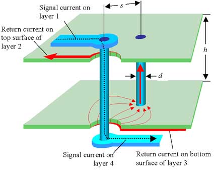
On high-speed designs, each of your signals is going to seek a route from source to sink along the path of least impedance. For system clocks and other high-speed I/O devices, ensuring this smooth path of travel might require the use of a via. Without these, you might find yourself with currents spreading around splits in your ground plane, and in turn, leading to a loss of signal integrity.

If you do find yourself using vias to return your currents to their termination, then make sure you use tightly coupled, impedance-matched differential vias. This will ensure your signals arrive on time. And when placing your return vias, place them as close as possible to your signal vias to minimize the length your signal has to travel.
8. Use the 3W Rule to minimize coupling between traces
Having your transmission lines couple can spell bad news for the integrity of your signal in transit. And while there’s always the general rule of keeping traces as far apart as possible to minimize this risk, it gets a bit fuzzy when it comes to the execution.
If you’re wondering how far you need to keep your traces from each other to minimize coupling, then use the 3W Rule. It states that the separation between traces must be three times the width of a single trace when measured from center to center. You can also increase this separation from three to 10 times to get even greater gains on reducing coupling and crosstalk.

9. Use the 20H Rule to minimize plane coupling
In addition to the risk of coupling for individual traces, you also have to worry about the coupling between power and ground planes on your layout. If these two couple, you’ll get RF radiation spilling off the edges of your board, called fringing.
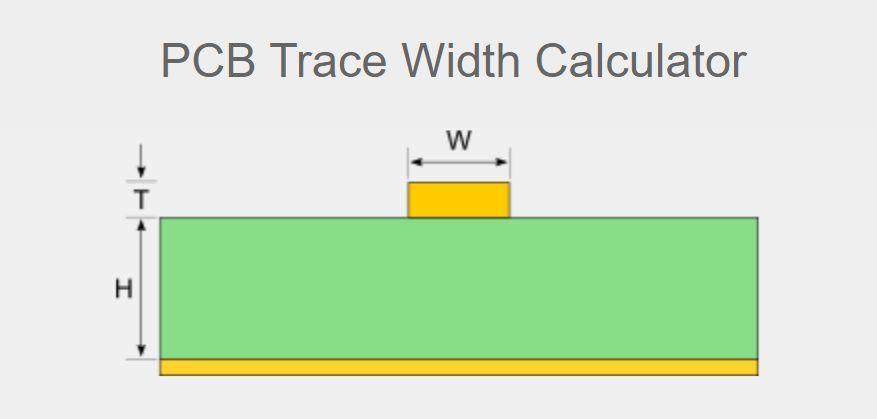
To prevent this from happening, you’ll want to make any power plane that is adjacent to a ground plane smaller than the ground plane. This will allow any fringing to be absorbed into the ground plane instead of radiating out externally. How much smaller, though? Use the 20ᐧH rule, which says to make your power plan 20 times smaller than the dielectric thickness between your adjacent power and ground planes.

10. Finishing with general routing guidelines
In comes routing to finish off our top 10 tips! Routing really deserves a blog post and book of its own to address things like RF, microwave, or antenna design. This list isn’t exhaustive, so be sure to seek out the advice of a seasoned engineer for application-specific routing techniques. Here we go:
- 90-degree no-no. The first is always to avoid using 90-degree angle bends in your traces. Right-angled traces can lead to signal reflections.
- Differential pairs. You’ll only get the benefits of electromagnetic field cancellation when both the signals in your differential pair have the same length and gap. This will likely require some length match tuning in your PCB design software.
- Transmission lines. Take the time to carefully design your transmission lines with the use of microstrip or stripline traces. Microstrip traces will only provide one reference plane separated by a dielectric. If you need more shielding capabilities, then a stripline will place a trace between multiple ground planes and a dielectric.
High-speed PCB design with Fusion 360
Now you’re ready to start diving deeper into the world of high-speed design! Soon enough, you’ll start combating EMI with EMC or electromagnetic compatibility with a 1, 2 punch. There’s still so much to learn. So consider these top 10 tips as just the basics to get you started on your first project!
Check out this three-part series to learn more about high-speed PCB design in Fusion 360:
Ready to begin your first high-speed design project? The Autodesk Fusion 360 Signal Integrity Extension has all the tools you need and much more. Get started for free today:
