Learn what PCB vias are, specifically blind vias, buried vias, and micro vias are and how they play a particularly important role in PCB design.
What are PCB vias?
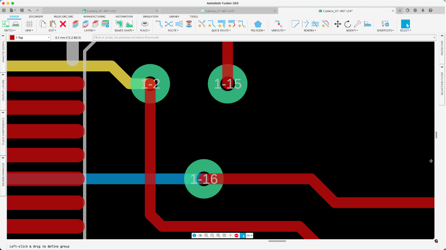
PCB vias (Vertical Interconnect Access) are small, copper-lined hole drilled through one or more layers of a printed circuit board. It creates an electrical connection between different layers, allowing signals and power to pass vertically through the board, which is essential for complex, multi-layer PCB designs.
The importance of PCB vias
In the world of printed circuit board (PCB) design, vias play an essential role in ensuring the efficient transfer of electrical signals between different board layers. The complexity of modern electronics and the increasing density of components in PCBs necessitates using various types of vias. Among these, blind vias, buried vias, and micro vias are particularly important. This article explores the differences between these three types of vias and their respective applications in PCB design.
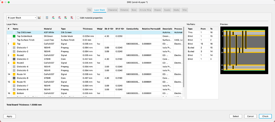
What are blind PCB vias?
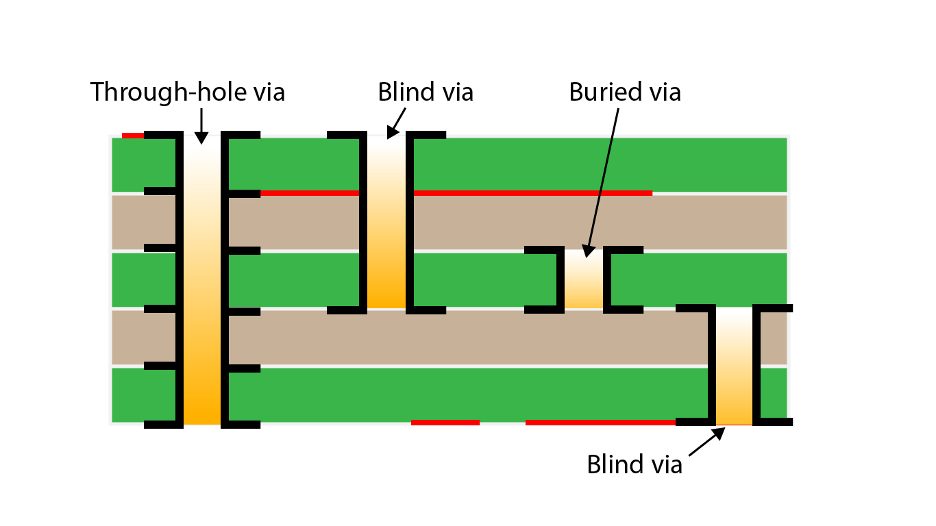
Blind vias connect an outer layer of a PCB to one or more inner layers without penetrating the entire board. As the name suggests, these vias are “blind” because they are not visible from the opposite side of the PCB. Blind vias offer several advantages, such as saving space on the board, enabling more compact designs, and improving signal integrity by reducing the length of signal paths.
Blind vias are drilled through the PCB’s surface layer and only extend a portion of the way through the board, linking the surface layer to one or more inner layers. They are a crucial component in current PCB design, allowing surface-layer components to be connected to inside layers while minimizing the number of layers necessary for routing.
Advantages of using blind vias
- Increased density: By linking surface-mounted components to inner layers, blind vias enable more efficient use of board space. As a result, the overall size and weight of the PCB may be reduced.
- Reduced layer count: Blind vias can assist in minimizing the cost of PCB manufacture by lowering the number of layers required for routing.
- Improved signal performance: Signal routing over blind vias can reduce crosstalk and EMI between traces, improving signal quality and reliability.
- Drawbacks of using blind vias include:
- Manufacturing difficulty: Blind vias necessitate accurate drilling and plating operations, which can raise Board manufacturing costs and complexity.
- Layer count restrictions: Blind vias have the potential to reduce the number of layers that can be employed in a PCB design.
Examples of PCB designs that make use of blind vias
Smartphones, laptops, and other portable electronic gadgets, which require high-density PCB layouts to accommodate many components into a small space, are examples of PCB designs that use blind vias.
Blind via manufacturing considerations
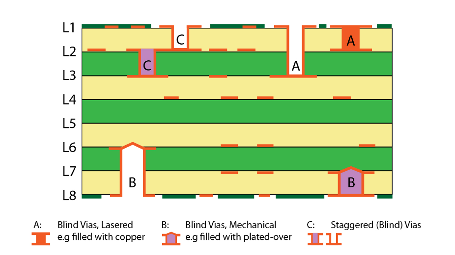
Blind through hole production challenges include the necessity for accurate drilling and plating operations, which might raise manufacturing costs. Although laser drilling technology can enhance precision and save costs, it may only be appropriate for some PCB designs.
The aspect ratio of the vias, which is the ratio of the diameter to the depth of the via, must also be considered by designers. Larger aspect ratios might be more challenging, increasing costs and possible manufacturing problems.
Applications of blind vias include high-density interconnect (HDI) boards, where space is at a premium, and high-speed digital circuits, where signal integrity is crucial. Blind vias are typically more expensive to manufacture than through-hole vias, but their benefits often outweigh the added cost in demanding applications.
What are buried PCB vias?
Unlike blind vias, buried vias connect two or more inner layers of a PCB without any connection to the outer layers. They are entirely hidden within the board and cannot be seen from either side. This feature allows designers to use the outer layers of the board for other purposes, such as placing components or routing traces, without interference from Vias.
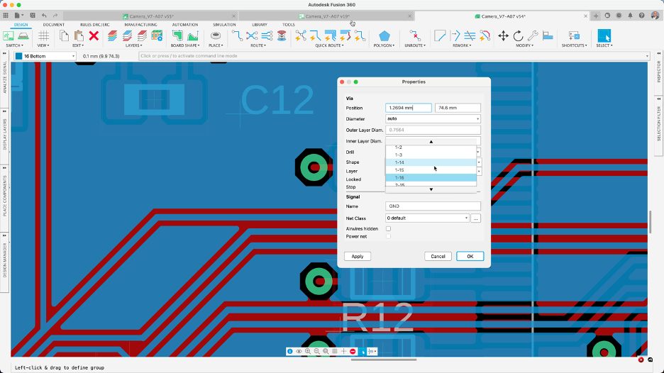
The primary advantage of buried vias is the increased density they enable in PCB designs. This is particularly useful in multilayer PCBs, where space for routing traces and placing components is limited. However, the production of buried vias is more complex and costly than through-hole vias, requiring additional manufacturing steps such as sequential lamination and drilling.
Advantages of using buried vias
- Increased density: Buried vias, which connect the inner layers of the PCB without extending to the top layers, can help enhance the density of components on the board.
- Reduced layer count: Buried vias can assist in reducing the number of routing layers necessary, resulting in lower manufacturing costs.
- Improved signal performance: Signal routing through buried vias can reduce crosstalk and EMI between traces, improving signal quality and reliability.
Drawbacks of using buried vias
- Manufacturing difficulty: Buried vias necessitate accurate drilling and plating operations, which raises the cost and complexity of PCB production.
- Accessibility issues: Because buried vias are not visible from the board’s surface, they might be challenging to troubleshoot and repair if they fail.
- Examples of PCB designs that make use of buried vias
- High-density computing, telecommunications equipment, industrial control systems, and medical devices are examples of PCB designs that incorporate buried vias.
- Buried via manufacturing considerations The need for precise drilling and plating operations, which might increase production costs, is one of the manufacturing considerations for buried vias. The aspect ratio of the vias, which is the ratio of the diameter to the depth of the vias, must also be considered by designers.
Larger aspect ratios might be more challenging, increasing costs and possible manufacturing problems. It is also critical to verify that the needed number of buried vias has enough space on the board and does not interfere with other components or traces.
What are micro PCB vias?
The miniaturization of electronic devices has led to increased demand for more compact and efficient printed circuit board (PCB) designs. To meet these demands, designers have turned to using micro vias, which are small vias with a diameter of 150µm or less.
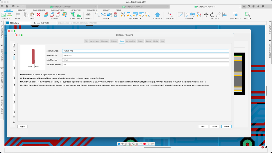
Micro vias are tiny holes drilled into printed circuit boards (PCBs) to connect the various layers of the board. Lasers are commonly used to drill these holes, which have a diameter of fewer than 150 microns and are extremely precise. Their capacity to enhance circuit density while reducing board space is mainly responsible for its meteoric popularity over the past few years.
They are commonly used in high-density interconnect (HDI) PCBs to connect very fine-pitch surface-mount components, such as ball grid array (BGA) and chip-scale package (CSP) devices. The small size of micro vias allows for higher routing density and better signal integrity in these demanding applications.
Micro vias manufacturing typically involves laser drilling or other advanced techniques, which can be more expensive than traditional drilling methods. However, the improved performance and reduced board size achieved with micro vias often justify the additional cost.
Stacking micro vias can further optimize PCB designs by improving density and performance. The following discusses the effects and applications of stacked micro vias in PCB designs.
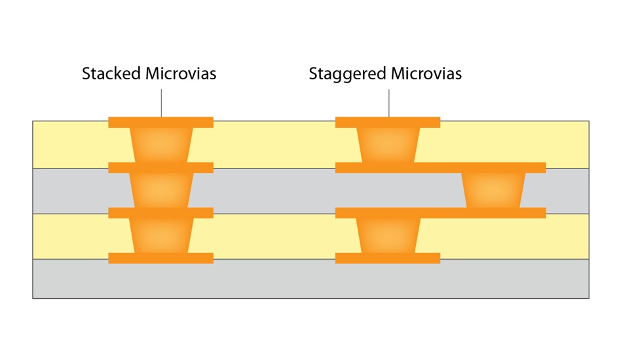
These microscopic, laser-drilled interconnects enable designers to achieve complex, multi-layered designs within compact spaces. As a result, stacked micro vias have transformed the electronics industry, providing numerous benefits that range from size reduction to improved signal integrity.
Stacked micro via benefits
Signal integrity is critical for high-speed digital circuits and communication systems. Stacked micro vias improve signal integrity by providing a shorter, more direct path for electrical signals to travel between layers, reducing parasitic inductance and capacitance. These results can lower signal reflection and attenuation, improving overall performance in high-speed applications.
As electronic devices become smaller and more powerful, efficient thermal management becomes increasingly important. Stacked Micro vias facilitate better heat dissipation. By creating a network of micro vias or thermal vias, heat can be transferred from the heat source to other layers of the PCB, which can help dissipate the heat and prevent localized hotspots.
Advantages of using micro vias
- A higher number of circuits per unit area: Because micro vias make it possible to make more connections in a smaller area, this can increase the number of components placed on a printed circuit board (PCB).
- Improved signal integrity: Micro vias has the potential to shorten the length of interconnects, which in turn will result in less signal loss and greater signal integrity.
- Lower cost: Micro vias can potentially lessen the number of layers necessary for a printed circuit board, lowering the production cost.
Drawbacks of using micro vias
- Increased complexity: Adding micro-vias to a PCB design can complicate building and troubleshooting.
- Decreased dependability: Because of their smaller size, micro vias can potentially have more failures than regular vias. Issues such as poor plating quality, inadequate hole fill, and voids in the via can occur during the fabrication process, which can impact the reliability of the stacked micro vias. These issues can lead to electrical opens or shorts, signal integrity problems, and reduced overall reliability of the PCB.
Micro vias are used in the following PCB designs
It is common to practice incorporating micro vias into high-density printed circuit board (PCB) designs, such as those utilized in smartphones, tablets, and other portable electronic devices. They are also used in high-speed digital and RF applications, both of which place a significant emphasis on maintaining signal integrity.
Considerations when constructing printed circuit boards (PCBs) with micro vias
- Drilling: Drilling micro vias often involves using a laser, which necessitates precise manipulation of the laser’s settings to guarantee that the resulting holes have the appropriate size and shape.
- Plating: To guarantee that micro vias are correctly connected to the other printed circuit board (PCB) layers, particular plating procedures must be utilized.
- Inspection: Because micro vias might be challenging to verify visually, non-destructive testing techniques may be necessary to guarantee that they are produced and connected appropriately.
- Material selection: The reliability of micro vias can be significantly impacted by the materials selected for use on the printed circuit board. For micro vias to be reliable, the materials used in their construction must be of a high grade.
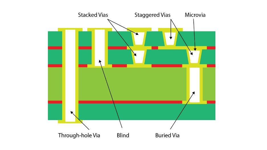
The similarities and differences between blind, buried, and micro vias
Similarities
- Blind, buried, and micro vias are all designed to save space on the PCB compared to traditional through-hole vias. They can provide a more efficient use of board real estate, allowing for increased component density and more complex PCB designs.
- There types of vias are designed to allow for higher-density interconnects, providing more routing options in high-density designs.ds
- Compared to traditional through-hole vias, all three types of vias are smaller in size, typically with diameters ranging from a few microns to a few tenths of a millimeter.
- Blind, buried, and micro vias all require specialized fabrication techniques, such as laser drilling and plating, to create the desired via structures. This requires additional manufacturing steps and expertise, which can increase the cost and complexity of the PCB manufacturing process.
- Depending on their placement and routing, all three types of vias can potentially impact signal integrity. Careful consideration of via placement and routing is necessary to minimize signal integrity issues.
Differences
- In a printed circuit board (PCB), a buried via connects two or more inner layers without reaching the outer layer. In comparison, a blind via connects the exterior layer about one or many middle layers.
- Micro vias are a more compact alternative to blind and buried vias and connect neighboring ring layers.
- Micro vias are drilled from the middle of the board, while blind and buried vias are drilled from either the top or bottom of the board.
- The production of buried vias is typically more challenging, time-consuming, and expensive than the production of blind or micro vias.
Choose the best via for your PCB layout
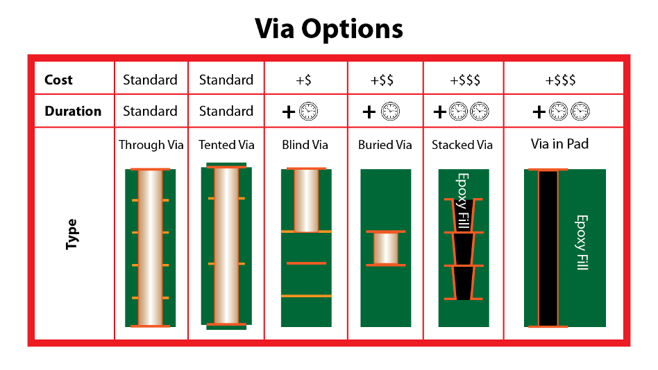
Tented vias are a type of via in printed circuit boards (PCBs) where the via holes are covered or “tented” with solder mask during the PCB manufacturing process. This means that the via holes are fully coated with solder mask material, a protective layer applied over the copper traces on the PCB to prevent solder bridging, short circuits, and other manufacturing and assembly issues.
Before deciding on the type of material to be used in designing a printed circuit board (PCB), it is crucial to consider numerous distinct issues seriously. This choice is required before the PCB can be manufactured. Such considerations have been implemented on the PCB.
- The required density
- The number of board layers
- Signal speed,
- and the available budget is all factors to be considered while making this selection.
Blind and buried vias are more suited to high-density systems with many layers, while micro vias are more appropriate for designs with fewer layers and smaller components. An increase in the prevalence of blind and buried vias has also been observed.
Micro vias are most useful in designs with few layers and small parts. Micro vias are most useful in designs where the number of layers is low, and the components are relatively small. Regulated impedance is essential for high-speed communications; therefore, more than one type of via will likely be needed.
Blind, buried, and micro vias are essential tools in the PCB designer’s arsenal, enabling the creation of compact, high performance, and high-density boards. While they may come with additional manufacturing costs, these specialized vias are indispensable in meeting the demands of modern electronics. By understanding the differences and applications of each type of via, designers can optimize their PCB designs and achieve the best performance in their electronic products.