What Is Differential Signaling, and Why You Need It For Your High Speed PCB Design?
There’s something awesome about being able to use the latest technologies and interfaces in your PCB design. We’re talking about things like USB 3.0, HDMI, Ethernet; the list goes on. Anything that adds some modern day functionality to your device and makes it stand out. But there is a tradeoff when adding some of these advanced technologies onto your board; they suddenly throw you into the world of high speed design. It’s in this world where you have to pay attention to more variables than ever, like signal integrity (SI), electromagnetic interference (EMI), and most importantly, differential signaling. While you might have been using single-line traces in the past, if you want to work with the latest technologies then prepare to add a paired trace to the mix. So what is differential signaling all about, and why would you ever need to use it on your high speed PCB design? Let’s find out.
What You’re Used To
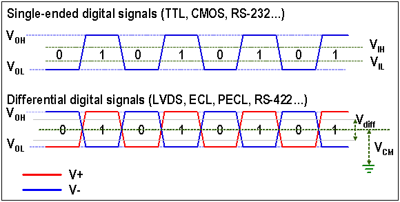
To understand differential signaling, you first have to understand its opposite – single-ended signaling. Don’t let the fancy name throw you off; this is exactly the kind of signaling you’ve been working with on any PCB design that isn’t considered high speed. As the name suggests, single-ended signaling is all about sending a signal from a transmitter to a receiver with one trace. That’s it.

This means that you’ll have a single copper trace carrying your signal to its end destination, and from there it heads to your common ground and back to your source. This is a common practice in every standard PCB layout you might have worked on in the past. Anytime you draw a trace in Autodesk EAGLE and connect it from one pin to another; then you’re working with a single-ended signal.
When you start cramming in a bunch of traces and components into really tight spaces, then you need a way to work around potential electromagnetic interference (EMI) issues. Because if there’s anything to know about EMI issues, it’s that it will do an excellent job of messing up the quality of the signals that you’re sending. Here’s an example:
- Say you need to store a piece of data into a particular spot in DDR memory, so you send a signal from point A to point B.
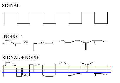
- What happens along this signal’s journey if it encounters some electromagnetic interference? The data inside the signal may be affected by the interference. Turning our nice beautiful square wave into a fuzzy mess.
- And before you know it, the signal you sent ends up all jumbled and unrecognizable.
To help protect the integrity of signals along their journey in a high speed design, you need a more robust way to keep your information-in-transit secure than what single-end signaling can provide. And this is exactly what differentials signaling help shield.
What Differential Signaling Is All About
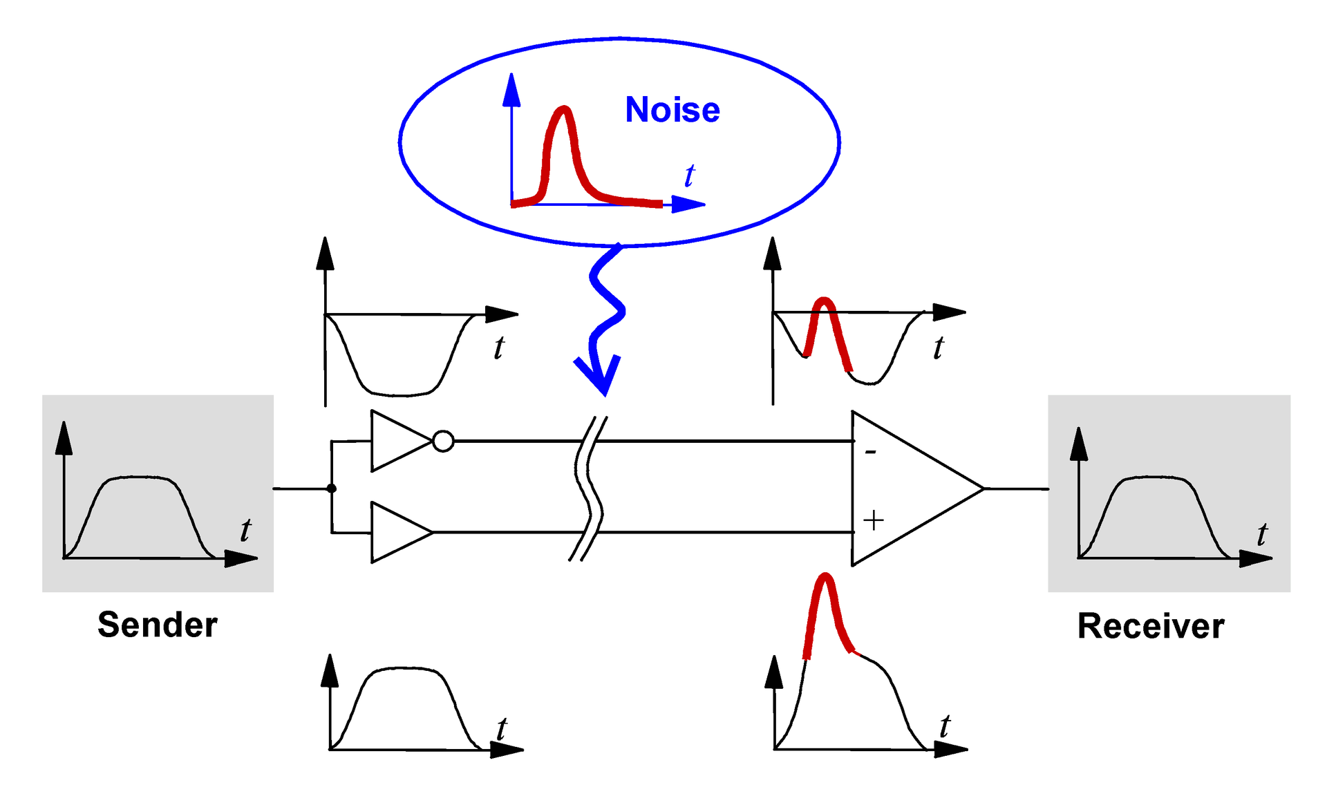
Unlike single-ended signals, differential signals take advantage of not one, but two traces that work in tandem together. Here’s how it works – you’ve got two traces that both carry the same signal, one of which is considered the positive signal, and the other trace is considered the negative signal.

When information is transmitted along this dual-trace arrangement and arrives at its destination, a receiver can then extract the data by analyzing the potential difference between the positive and negative signal. And by analyzing this dual signal and its voltage difference, your receiver can go about understanding whether this signal is transmitting a 1 or a 0, or a high or low voltage.
So for every differential signal that you need to add on your board, you’ll need to have two traces lined up side-by-side. For example, if we have a board with 20 different nets that need to be connected, we’d need a total of 40 individual traces to get the job done.
We know what you might be thinking now – why in the world would I ever want to double the amount of traces on my board layout? That’s going to take up some valuable real estate on a PCB that could be used for component placement and making my routing job easy. At a glance you’re right, differential signals do take up more space on your PCB, but they have some convenient benefits in high speed design applications, such as:
Keeping Power Systems Separate
Because differential signals are equal and opposite, they don’t necessarily send a return signal to ground; then you can make something like an analog signal going to a digital device without having to worry about crossing over power boundaries. This makes it a lot easier to keep power systems separate. One thing to bear in mind though, if you’re working with USB or RS-485 technologies, then you’ll most likely need a shared ground so that your differential signals stay within the required voltage threshold.
Resisting Incoming Electromagnetic Interference
Differential signaling also has the added benefit of reducing any incoming electromagnetic interference or crosstalk from other noisy traces. Any interference that a differential signal soaks in gets distributed evenly between the positive and negative traces, which reduces any change in amplitude that external EMI issues can cause.

Resisting Outgoing Electromagnetic Interference
Your differential signals will also generate their own EMI while transmitting information, just like single-ended signals. However, because the positive and negative signals in a differential share the same polarity and distance, this effectively cancels out any EMI emissions.

Lower Voltages
Differential signals also have the added benefit of being able to operate at lower voltages than single-ended signals, all while maintaining their signal-to-noise ratio (SNR). And with lower voltages, you get the benefit of being able to use lower supply voltages, reduced power consumption, and reduced EMI emissions.
Timing Precision
Single-ended signals have a bunch of factors to consider to determine what kind of logic state they might be in, like the power supply voltage, reference voltage, etc. But with differential signals, this is a lot easier to determine. If the negative trace in a differential signal is a higher voltage than the positive trace, then you have a high logic state, and if it’s the other way around, then you have a low logic state.

Using Differential Signals In Your Design
Now that you understand all of the great benefits that come with using differential signaling on your high speed design, you might be wondering what kind of constraints they require. As you can probably imagine, all of the benefits of differential signaling weighs heavily on being able to keep those traces at a consistent length and space from each other at all times, otherwise, you’ll mess up the equal voltage and polarity benefits between the two. Here are three quick tips when setting up the design rules for your differential signals in Autodesk EAGLE:
- Rule 1 – Keep your traces at equal lengths. If you don’t do this, then you ruin the entire benefit of two traces being coupled together along their entire transmitter to receiver journey. And losing that means dealing with some nasty EMI emissions that can corrupt your data. In most devices, you can have a trace length difference of up to 500 mils tolerance but keep them as close as possible.
- Rule 2 – Route differential traces close together. Called coupling, this again comes down to a concern about EMI. The closer that you route your differential signals together, the smaller you make the loop area of your induced current, which has a direct impact on how much EMI your traces will emit. By keeping two traces close together, your ability to cancel out EMI issues is greatly enhanced.
- Rule 3 – Keep your impedance consistent. It’s important to always keep your differential trace impedance constant over the entire length of its venture from the transmitter to the receiver. Your impedance will depend on many things, like the width of your traces, the thickness of your copper, and the materials you’re using in your layer stack up. Dial down these variables, calculate exactly what you’re impedance needs to be, and stick with it.
Staying With the Times
If you’re going to be working with the latest technologies on your PCB design like USB 3.0, HDMI, DDR, Ethernet, etc. then differential pairs are going to be your new best friend. Not only do these tightly coupled traces help to reduce incoming and outgoing EMI, but they also make it easy to keep power systems separate, and can lower the overall voltage needed to power your project. Remember though, to get all of the benefits of differential signaling you need to strictly define your design rules to keep your traces at equal lengths with tight spacing and exact impedances. If you don’t, you’ll ruin their beneficial balance!
Ready to get started with differential signaling on your first high speed design project? Try Autodesk EAGLE for free today!