Electronic circuit design involves ideation, creation, and revision. Learn about PCB design and the circuit design process.
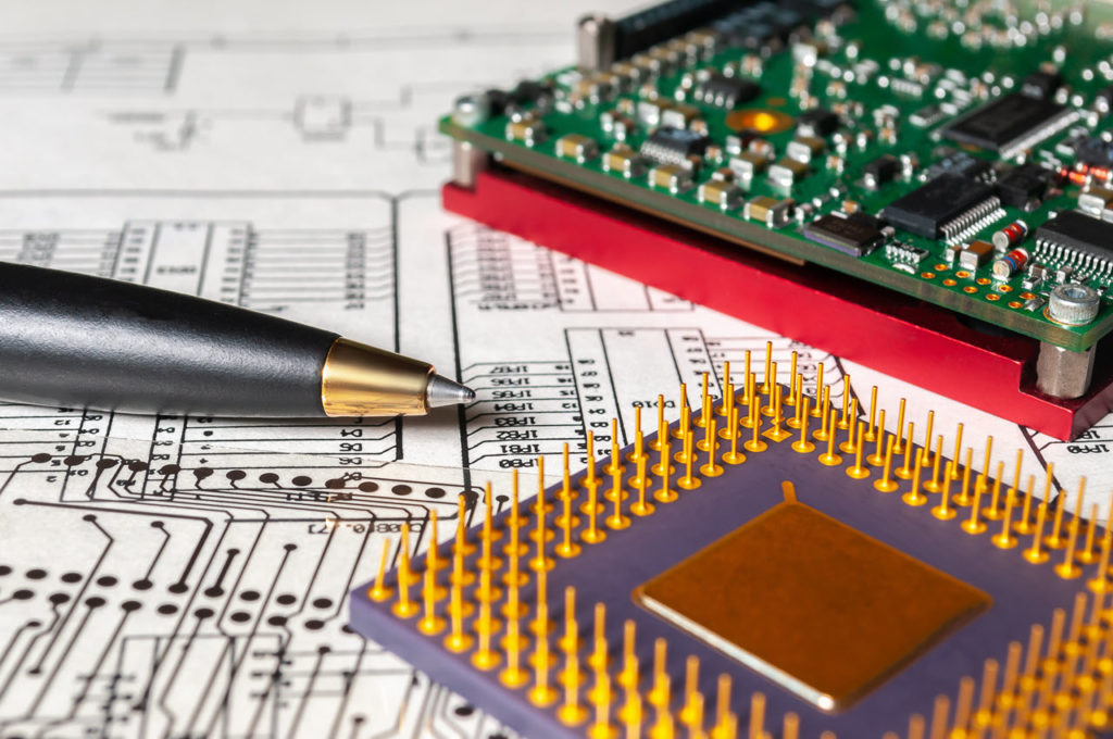
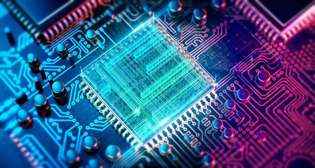
Printed Circuit Boards (PCBs) are in every piece of modern electronic equipment, which is why it’s important to know what, exactly, a circuit board consists of and how designers can implement it into so many applications.
Designing an electronic circuit begins on the breadboard (protoboard). The bedboard is a thin plastic rectangular construction base to which electronic components are soldered. The soldered connections are not permanent and can be removed and placed again and again within reason. The construction of a breadboard subsequently turns it into what is known as a PCB, often used in computations, signal amplification, and data transfer.
The interconnections on a PCB connect the soldered components. Charge flows from the positive terminal throughout the interconnection loops to the negative terminal.
The Basics of Electronic Circuit Design
Integrated circuits (ICs) have vastly improved metal-oxide-semiconductor field-effect transistors (MOSFET). There are three common circuit designs: analog, digital, and mixed-signal.
Analog Circuit Design
Analog circuit designs generally consist of diodes, transistors, transformers, operational amplifiers, and other passive components. These circuits perform complex data analyses, filtering, and amplification.
Digital Circuit Design
Digital circuit design functions on discrete values (zeros and ones). These are usually part of the whole PCB design.
Mixed Circuit Design
In many modern applications, PCB designers rarely use just analog or digital circuit layouts. Digital and analog circuits are separated to reduce noise and improve performance.
Microcontroller
Microcontrollers are integrated digital circuits that you can program to perform a variety of commands.
Field Programmable Gate Arrays (FPGA)
FPGAs are digital circuit boards that you can directly configure on a hardware level instead of using a set of instructions. FPGAs are best used for high-performance systems such as aerospace applications.
Schematic Circuit Diagrams
A schematic circuit diagram represents components and interconnections in a PCB layout. These typically use standardized symbols and are two-dimensional and are often used in construction and electrical maintenance.
The Circuit Design Process
The circuit design process is extensive — it involves ideation, testing, prototyping, revising, and retesting. Circuit design goes through several iterations like the writing process, before achieving a final product. Both processes begin with an outline or preparation of the idea.
Outlining
Outlining is one of the most important aspects of circuit design. Outlining is where the designer prepares the architecture of the PCB. Specialty components like integrated circuits are selected during this stage.
Schematic Drawing
Once complete, the outline is translated onto a schematic where components are connected to achieve circuit functionality. This process usually involves many components, modules, and subcircuits.
PCB Layout
In this stage, the PCB drawing is now a PCB layout initiated by transferring components into the schematic. The schematic is checked for errors, and the revision process begins. It’s not uncommon for components to rearrange to solve schematic errors or design rule violations.
Prototyping
Prototyping involves fabricating the PCB in small volumes to ensure functionality. You should document design errors and schedule for revision during the next round of layout changes.
Component Placement
Depending on the manufactured prototype, components are placed on the PCB. For example, analog components must have adequate clearance from their high-speed digital counterparts. Component placement should alleviate future servicing and troubleshooting. In a way, this is designing for accessibility. It should be less complicated to service the PCB after several component placement revisions.
Electromagnetic Interference (EMI) Check
EMI should be checked at an increasing rate. This is due to electronics getting smaller, faster, and wireless. The best solution to EMI problems is properly separating ground planes to accommodate high-speed signals.
Power Delivery Network
Power modules are the lifeblood of the PCB. Thus, a bad power module could easily sink an otherwise perfect PCB design. A good power delivery network ensures minimal power loss.
Autodesk Fusion 360 gives you access to comprehensive electronics and PCB design tools in a software solution. Get started today with a 30-day free trial.