Ever wonder what a Field Effect Transistor (FET) is? Give this article a read for everything you need to know about the device.
What is a Field Effect Transistor (FET)?
A Field Effect Transistor (FET) is a three-terminal Active semiconductor device, where the output current is controlled by an electric field generated by the input voltage. FETs are also known as unipolar transistors because, unlike bipolar transistors, FETs only have either electrons or holes operating as charge carriers. FET uses the voltage applied to its input terminal (called the Gate), to control the current flowing from the source to drain, making the Field Effect Transistor a “Voltage” operated device.
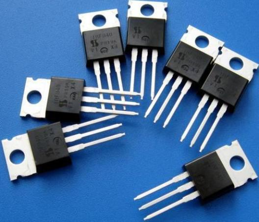
FETs are extensively used in Integrated Circuits (ICs) due to their compact size and significantly lower power consumption. Apart from that, FETs are also used in high power switching applications, as voltage-variable resistors (VVRs) in operational amplifiers (Op-Amps), and tone controls, etc., for mixer operation on FM and TV receivers and in logic circuits.
Elevate your design and manufacturing processes with Autodesk Fusion
Field Effect Transistor (FET) – Psychical Overview
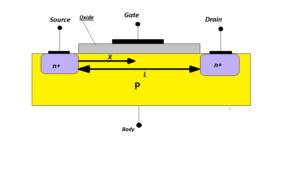
The Four Terminals of a FET: Source, Drain, Gate, and Body
- Source: Source is the terminal through which the majority charge carriers are entered in the FET.
- Drain: Drain is the terminal through which the majority charge carriers exit from the FET.
- Gate: The gate terminal is formed by diffusion of an N-type semiconductor with a P-type semiconductor. This creates a heavily doped PN junction region that controls the flow of the carrier from source to drain.
- Body: This is the substrate on which the FET is built. In discrete applications, it is internally tied to the source pin allowing its effects to be ignored entirely. However, in integrated circuits, this pin will be typically connected to the most negative power supply in an NMOS circuit(most positive in a PMOS circuit) because many transistors will share it. Careful connections and design are critical to maintaining FET performance when the Body connection is involved.
Channel: This is the region in which the majority carriers pass from the source terminal to the drain terminal.
FET Classification
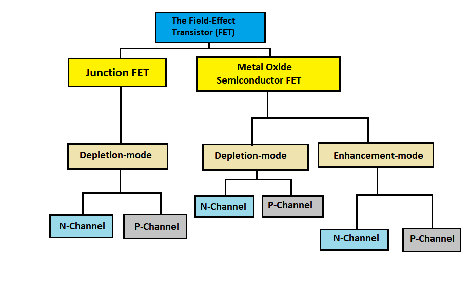
FET transistors are classified into:
- Junction Field Effect Transistors (JFET)
- Metal-Oxide-Semiconductor Field-Effect Transistors (MOSFET)
JFET (Junction-Field Effect Transistor)
The Junction Field Effect transistor (JFET) is the earliest type of FET. The current flows through an active channel between sources to drain terminals. The voltage applied between gate and source controls the flow of electric current between the source and drain of the JFET. By applying a reverse bias voltage to the gate terminal, the channel is strained, so the electric current is switched off completely. That is why JFETs are referred to as “normally on” devices. The JFET transistors are available in both N-channel and P-channel types.
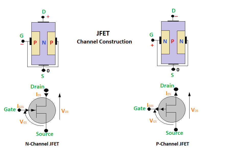
N-Channel JFET
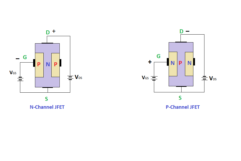
In the N-channel JFET, the channel is doped with donor impurities, making it an N-type semiconductor. Therefore the flow of current through the channel is negative in the form of Electrons. Hence the name N-channel JFET. Two P-type substrates doped at the opposite sides of its middle part. Thus two PN junctions are formed by those heavily doped P-type regions and the N-type channel in between. The gate (G) lead is connected internally to both the P-type terminals, while the drain (D) and source (S) leads are connected to either end of the N-type channel.
How does it work?
When no voltage is applied across the gate terminal, the channel becomes a wide-open path for electrons to flow. Therefore maximum current flows from the source to the drain terminal. The amount of current flow is determined by the potential difference between source and drain terminals and the internal resistance of the channel.
But the reverse thing happens when a negative voltage is applied to the gate terminal with respect to the source terminal, making the P-N junction reverse biased. A depletion region is created in the channel that makes the channel narrower, increasing the channel resistance between the source and drain, and the current flow becomes less.
P-Channel JFET
Similarly, in the P-channel JFET, the channel is doped with acceptor impurities, making it a P-type semiconductor. Therefore the flow of current through the channel is positive in the form of Holes. Hence the name P-channel JFET. The opposite side of the channel is heavily doped with N-type substrates. Like in an N-channel JFET, the gate terminal is formed by joining the N-type regions at both sides. The source and drain terminals are taken from the other two sides of the channel.
The operating principle is also similar to an N-channel JFET. The only difference is that you need to provide a positive gate to source voltage to turn it off. However, N-channel JFET has a greater current conductivity due to lower channel resistance than their equivalent P-channel types, since electrons have higher mobility through a conductor compared to holes. This makes the N-channel JFET more efficient than their P-channel counterparts.
Characteristics
Here a JFET is biased through a DC supply, which will control the VGS of the JFET. We can control the applied voltage across the Drain and Source terminal by varying the VGS. From there, we can plot the I-V characteristics curve of a JFET.
The output characteristics of JFET are drawn between drain current (ID) and drain-source voltage (VDS) at a constant gate-source voltage (VGS), as shown in the following figure.
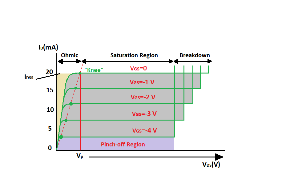
- Cutoff Region – This is the region where the JFET is off, meaning no drain current, ID flows from drain to source.
- Ohmic Region – In this region, JFET begins to show some resistance to the drain current, ID that is starting to flow from drain to source. The current flowing through the JFET is linearly proportional to the applied voltage.
- Saturation Region – When the drain-source voltage reaches a value such that the current flowing through the device is constant with the drain-source voltage and varies only with the gate-source voltage, the device is said to be in the saturation region.
- Breakdown Region – When the drain to source voltage, VDS exceeds the maximum threshold value, that causes the depletion region to break down, the JFET loses its ability to resist current, and the drain current increases indefinitely.
MOSFET (Metal-Oxide-Semiconductor Field-Effect Transistor)
Metal-oxide semiconductor field-effect transistors, also known as MOSFETs, have greater importance and are the most useful type among all transistors. The MOSFET has four terminals: drain, source, gate, and body or substrate. A MOSFET is also a voltage controlled Transistor, but the main difference between a JFET and a MOSFET is that it has a Metal-Oxide Gate electrode which is electrically insulated from the main current-carrying channel between the drain and source by a very thin layer of insulating material, usually silicon dioxide, commonly known as glass.
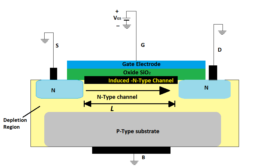
The track is made using two highly doped N-type zones diffused into a lightly doped P-type substrate. These two N-type regions are known as drain and source, and the P-type region is called the substrate. The isolation of the controlling Gate makes the input resistance of the MOSFET extremely high way up in the Mega-ohms (MΩ) scale, thereby making it almost infinite. Thereby no current is allowed to flow into the gate.
How does it work?
The main principle of the MOSFET device is to be able to control the voltage and current flow between the source and drain terminal using the voltage applied at the gate terminal. The semiconductor surface at the below oxide layer, which is located between the source and drain terminal, can be inverted from p-type to n-type by the application of either a positive or negative gate voltages, respectively. When we apply a repulsive force for the positive gate voltage, then the holes present beneath the oxide layer are pushed downward with the substrate. The depletion region is populated by the bound negative charges which are associated with the acceptor atoms. When electrons are reached, a channel is developed. The positive voltage also attracts electrons from the n+ source and drain regions into the channel. Now, if a voltage is applied between the drain and source, the current flows freely between the source and drain, and the gate voltage controls the electrons in the channel. Instead of the positive voltage, if we apply a negative voltage, a hole will be formed under the oxide layer.
Types of MOSFET
There are two MOSFETS widely used:
1. Depletion MOSFET:
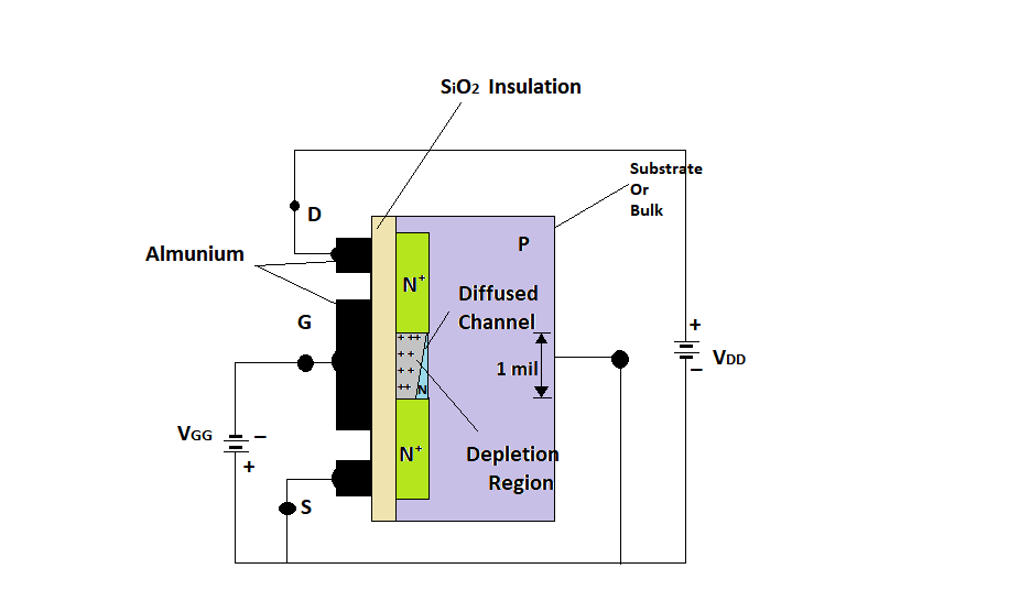
The depletion-mode MOSFET is similar to that of an open switch. In this mode, the Gate to Source voltage (VGS) is applied to switch OFF the device. When the gate voltage is negative, positive charges get accumulated in the channel. This causes a depletion region in the channel and prevents the flow of current. Thus as the flow of current is affected by the formation of the depletion region, it is called depletion MOSFET.
2. Enhancement MOSFET:
The enhancement-mode MOSFET is similar to that of a close switch. In this mode, the Gate-Source voltage (VGS) is applied to switch ON the device. When a negative voltage is applied to the gate terminal of MOSFET, the positive charge carrying holes get accumulated near the oxide layer, forming a channel from source to drain terminal. As the voltage gets more negative, the channel width increases and the flow of current enhances; thus it is called Enhancement MOSFET.
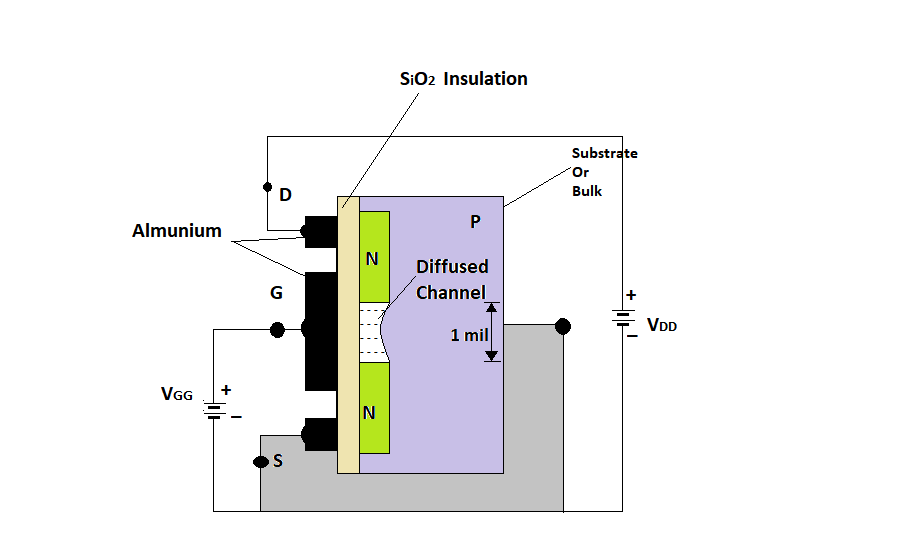
Further, the depletion and enhancement types are classified into N-channel and P-channel types.
1.N-channel MOSFET:
The N-channel MOSFET has an N-type channel between the source and drains terminal. Here the source and gate terminals are heavily doped with N-type semiconductor, and the substrate is doped with P-type semiconductor material. Hence the current flow between source and drain is because of electrons. And the current flow is controlled by the gate voltage.
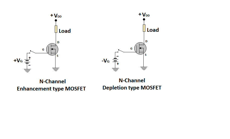
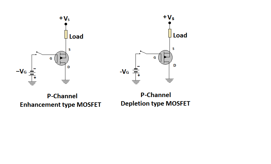
2.P-channel MOSFET:
Likewise, the P-channel MOSFET has a P-type channel between source and drain terminal. Here the source and gate terminals are heavily doped with P-type semiconductor, and the substrate is doped with N-type semiconductor material. Hence the current flow between source and drain is because of holes. And the current flow is controlled by the gate voltage.
Characteristics
In general, the operation of a MOSFET happens mainly in three regions and those are as follows:
- Cut-Off Region:
In the Cut-off region, the MOSFET remains OFF as there is no current flow in this region. Here MOSFET behaves like an open switch and is thus used when they are required to function as electronic switches. - Ohmic Region:
In Ohmic or linear region the drain to source current increases with an increment of voltage across the drain to source. When MOSFETs are operated in this region, they can be used as amplifiers. - Saturation Region:
In this region, the drain to source current value remains constant without considering the enhancement in the voltage across the drain to source. This happens only once when the voltage across the drain to the source terminal increases more than the pinch-off voltage. Under this condition, the device will act like a closed switch. Therefore this operating region is used whenever MOSFETs are required to perform switching operations.
Applications
MOSFET as a Switch
MOSFETs are used in many different applications. They are widely known for their switching characteristics. As we have seen earlier, an N-channel enhancement mode MOSFET has very high input resistance and operates on the positive input voltage. This allows us to switch high currents or high voltage loads, using a relatively low logic level signal. In the following example, we will use an Enhancement-mode N-channel MOSFET to switch a simple lamp ON and OFF.
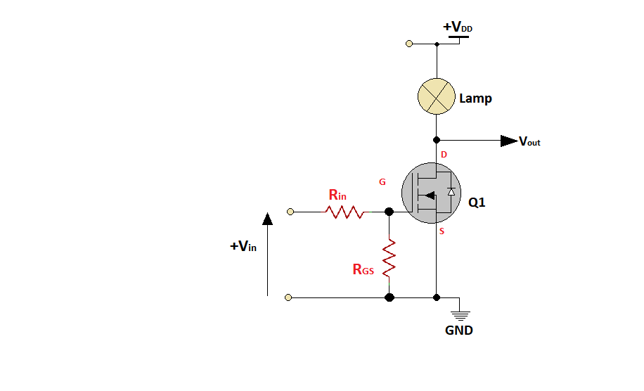
As you can see, in this setup, we want to switch a 12v lamp using 5v logic signal. We connected the positive terminal of the lamp to a 12v supply and the other end to the drain terminal of the MOSFET. The source terminal is connected to GND. A gate to source resistance (RGS) is used to avoid any external noise at the gate terminal.
When there is no voltage applied, the lamp will remain OFF condition. If we apply a positive input voltage (VGS) at the gate terminal of the MOSFET, the lamp will turn ON and remain ON until we remove the input signal or apply a negative input voltage. Then the lamp will turn OFF.
MOSFET Amplifier
Enhancement mode MOSFET or eMOSFET requires a minimum gate-to-source voltage, called the threshold voltage (VTH), that must be applied to the gate so that it starts to flow current from drain to source (VDS). As the forward bias of the gate increases, the drain-source current (IDS) will also increase, making the eMOSFET ideal for use in MOSFET amplifier circuits.
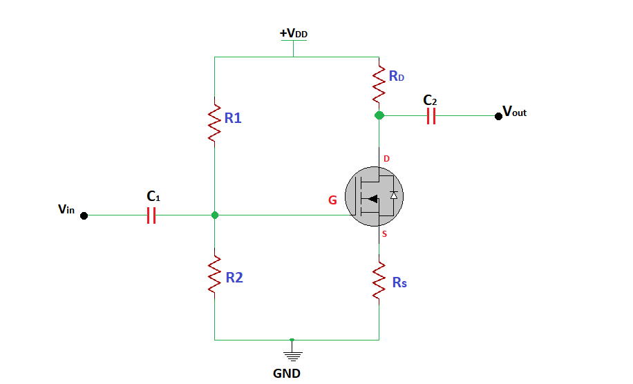
This simple enhancement-mode common source MOSFET amplifier configuration uses a single supply at the drain terminal to generate the required gate voltage (VG) using a resistor divider by the resistors R1 and R2. The resistor network creates the required biasing circuit to operate within its saturation region. We also need a drain and a source resistor and coupling capacities. The values of R1 and R2 are generally large in order to increase the input impedance of the amplifier and to decrease the ohmic power losses. The coupling capacitors C1 and C2 insulate the biasing DC voltage from the AC signal to be amplified. In the above image, a small AC signal (VGS) is applied to the MOSFET gate, resulting in a fluctuation of drain current synchronous to the applied AC input.
H-bridge Motor Driver
An H-bridge is a circuit configuration commonly used to control the speed and direction of a brushed DC motor. As we have seen earlier, using a MOSFET, we can easily control the speed of a motor. But that works only in one direction. In order to make it bidirectional, we need 4 MOSFETs connected in such a way that it can switch both the high side and the low side simultaneously.
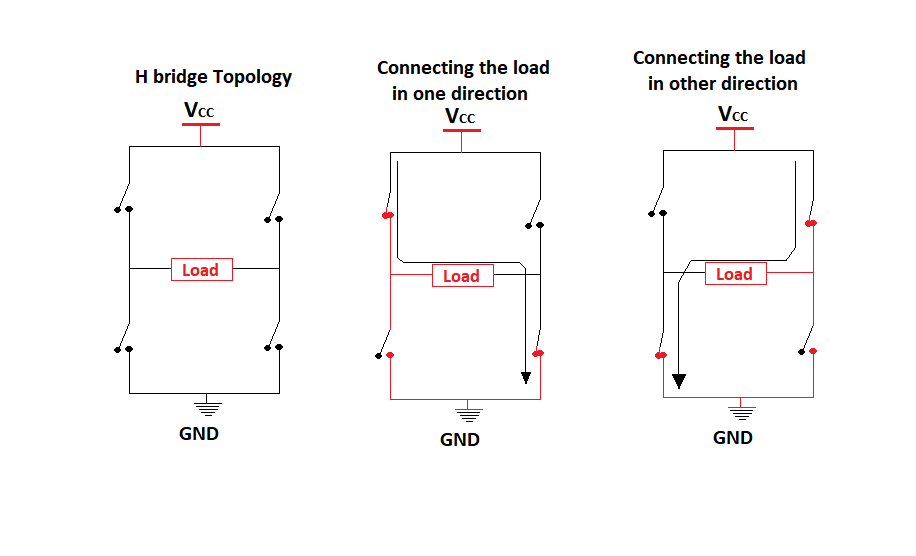
When activating one pair of (diagonally opposite) MOSFETs, the motor sees current flow in one direction, and when the other pair is activated, the current through the motor reverses direction. Triggering both the bottom and top MOSFETs (but never together) interrupts the current flow and stops the motor.
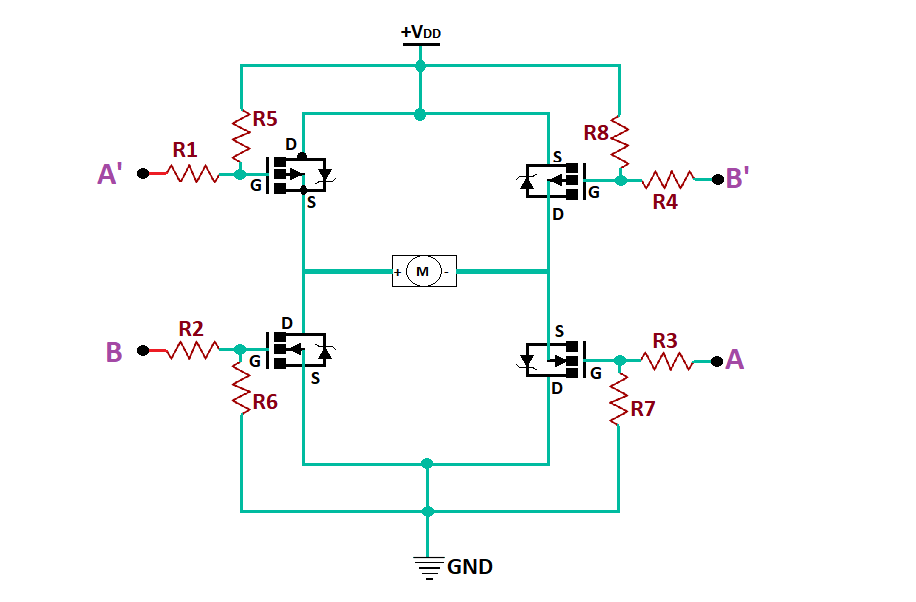
The N channel MOSFET gates are typically pulled low by the pulldown resistor, and the P channel MOSFET gates are pulled high. This results in both the P channel and the N channel MOSFETs are turned off; therefore, no current can flow. When the PWM signal is applied to the gates of the MOSFET, the N and P-channel MOSFETs have turned on and off alternately, controlling the power.
Field effect transisitor (FET) applications
Field effect transistor technology can be used in various fields of electronics, where bipolar transistors are not as suitable. The FET has a very high input impedance and is a voltage-driven device; they are possibly the most widely used active device. As they are used in CMOS and other integrated circuit technologies where power consumption is a crucial factor, MOSFETs enable very low power operation. A MOSFET can also be used as a switch to control bigger loads such as lamps or high power motors. PWM signals from an external source like a microcontroller are used to control the conduction of the transistor. Accordingly, the MOSFET switches on or off, thus maintaining the brightness of the lamp or speed of the motor.
Have you explored Fusion electronics capabilities yet? Fusion offers access to comprehensive electronics and PCB design tools in one product development platform on the cloud. Try it out for yourself today.
