Take an in-depth look at what exactly USB 3.0 is and the best routing practices involved in its PCB design.

What is a USB?
A Universal Serial Bus (USB) is an interface or a connectivity standard that almost everyone uses daily. You don’t have to be a tech geek to know how to connect two devices using a USB port. From computers to phones―this connectivity standard is used almost everywhere and has many types. Let’s learn about USB 3.0 and the best routing practices involved in its PCB design.
What is USB 3.0?
A USB is usually used to connect two devices. You must have seen USB ports in multiple peripheral devices, including mice, keyboards, printers, and scanners. The critical difference between USB 3.0 and its previous version, USB 2.0, is the maximum theoretical data transfer rate increase from 480 Mbps to 5 Gbps.
A less obvious but equally important point is that with version 3.0, USB will not only overclock but also become isochronous and full duplex, i.e., will gain the ability to receive and transmit data at maximum speeds independently.
USB 3.0 is the third major version and compared to earlier standards, it has several advantages, including:
- higher data transfer rates
- higher power efficiency
- greater device compatibility
Benefits of USB 3.0
The main benefit of USB 3.0 is its speed. Large files, including HD video and high-resolution pictures, transfer ten times faster than earlier versions. Moreover, it is far more efficient than other widespread networking technologies like Wi-Fi and Ethernet.
Additionally, since USB 3.0 connections can provide up to 4.5 Watts of electricity, your device may charge more quickly and function for extended periods.
USB 3.1, which offers users a significant increase in transmission speed, was released in July 2013. Later, in September 2017, USB 3.2 was introduced, providing even faster rates and more advantages.
Can 3.0 USB Ports Be Used with Older Devices?
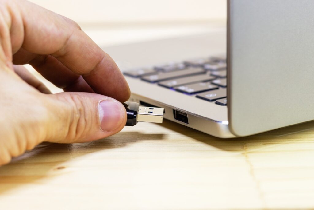
After learning about the latest version of USB, one might wonder about its compatibility with the older versions. Fortunately, USB 3.0 works with the earlier standards.
USB 3.0 and USB 2.0 devices supporting USB 2.0 can still communicate and work together. There are still certain restrictions, but the best part is that users won’t need to update their outdated peripherals and devices.
In particular, data transfer speed is limited to USB 2.0 levels, and USB 3.0’s increased power output is not supported. As a result, devices that need this power level won’t operate properly. Despite the drawbacks of using USB 3.0 with its older versions, the newer versions’ compatibility with the older ones is its key selling feature.
How Is USB 3.0 Different from USB 2.0?
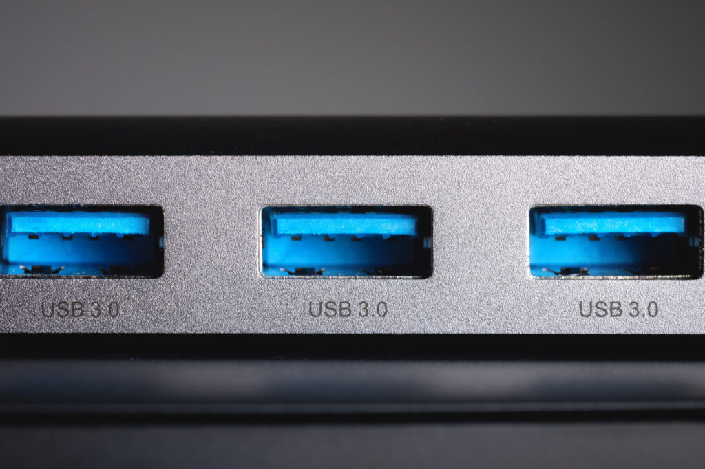
The significant difference between the two versions is speed. USB 3.0 offers a maximum speed of 5000 Mb/s, while USB 2.0 transfers data at 480 Mb/s. The considerable difference in rates makes the newer version better for specific applications. For example, USB 3.0 is superior for jobs like video editing or file backups that require the rapid transfer of huge volumes of data.
Power usage is another significant difference between these two models. Because USB 3.0 devices use less energy, they can run longer on a single charge. That is highly helpful for devices like laptops and smartphones.
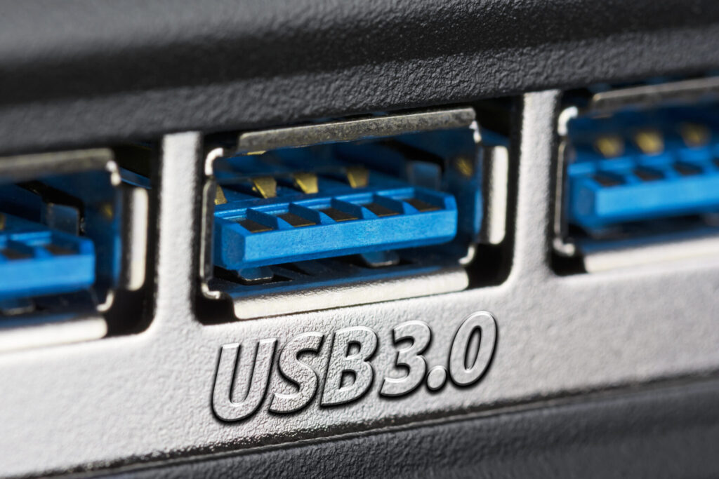
And finally, you can identify a USB 3.0 port by its appearance. Its teal blue plastic insert distinguishes itself from the black USB 2.0 ports and connectors. This makes it easier for consumers to differentiate between the standards and determine what is compatible with the USB ports on their computers.
Types of USB 3.0 Connectors

USB Type-A
USB 3.0 type-A ports and connectors are the most popular and recognized. They are on devices like smart TVs, gaming consoles, and PCs. Moreover, charging cables for computers, phones, and other portable devices also use this interface.
USB Type-B
Type-B connectors are less frequent and are typically used with electronics like external hard drives and digital cameras that need a more secure connection. In addition, they are frequently on large peripheral devices like printers and scanners.
USB Micro-A
Mobile devices like smartphones and tablets typically use the Micro-A USB 3.0 connector. It resembles Type A in shape but is significantly smaller, one-third the size. Despite its simple design, it still enables a fast transfer rate of up to 5000 Mb/s.
USB Micro-B
USB Micro-B differs from USB Micro-A and varies in size, but it has almost the same applications. It is used in external hard drives, GPS, and mobile devices.
USB 3.0: High-Speed Signal Routing
Trace Impedance
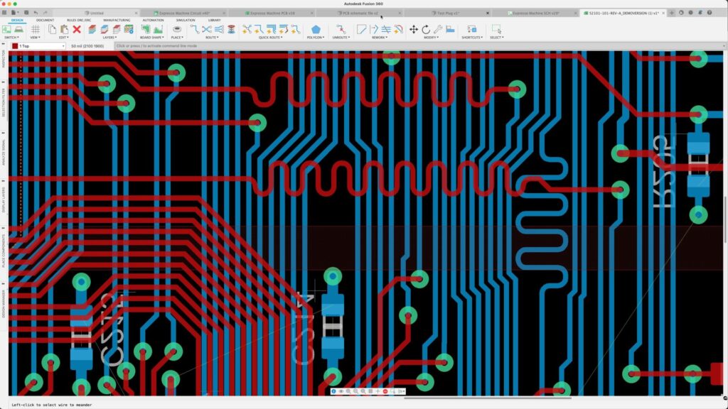
Now that we know how USB 3.0 works and what its applications are, let’s learn about the best practices involved in PCB designing involving USB. You may have seen circuit boards with USB connectors on them. While designing the PCB for such circuits, one must remember some rules and techniques to ensure smooth connectivity with minimum delays.
The trace impedance, total resistance, and reactance offered by a circuit path should be designed to minimize trace reflections when a high-speed signal passes through it. Typically, there are two types of trace impedances: single-ended and differential.
Single-ended impedance is the trace impedance compared to ground, while differential impedance is the impedance between two signal traces in a differential pair.
Another factor affecting the trace impedance is the high-speed protocol for making traces. It determines the single and divided trace impedance and the impedance tolerance. You should design the trace impedance near the recommended value for the best results. Moreover, the permittivity of the PCB material, the layers surrounding the trace, and the geometry of the traces all impact the signal trace’s impedance.
High-Speed Signal Trace Lengths
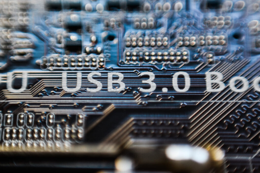
Maintain the shortest trace length for signal pairs, as with all high-speed transmissions. Some standards with maximum trace/cable lengths are listed in the various specifications.
Matching of High-Speed Signal Trace Lengths
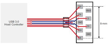
To match high-speed signal trace lengths, you must analyze the necessary differential pair traces, and their etch lengths and compare them. Before moving further, you must understand that the distinction between the etch lengths of the + and – lanes in a differential pair is known as ‘intra-pair skew.’ Meanwhile, the disparity between the etch lengths of one differential pair and another differential pair within the same group is referred to as ‘inter-pair skew.’
It is not necessary for the differential pair group’s etch lengths to coincide. In the USB 3.0, the TX and RX etch lengths do not have to match. Since the various lanes do not have to be the same length, specific standards do not have an intrapair skew requirement.
When modifying the intra-pair skew of the high-speed signals, add serpentine routing to suit the lengths as closely as possible to the mismatched endpoints.
Return Path
Every electrical circuit provides a return path for the current to flow back, making it part of a closed-loop system. The return path is the one with the least resistance. Since the reference plane next to the signal is often the lowest impedance path at higher frequencies, this path usually allows the return current to flow.

The layer above or below a signal layer is always preferable for a ground or power plane. This return path aids in minimizing EMI problems and impedance shifts.
High-Speed Signal Reference Planes
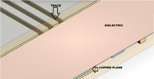
For high-speed signals, one must be careful about the ground reference plane. The ground plane for high-speed signals should be a solid one. It should not be a split plane or included as a reference plane under normal conditions.
While routing, you might have to do it over a split plane. It might seem like a simple task, but you should consider the path of the return current in this case. If your route over a void, it might create a longer feedback path for the current, which will give rise to multiple problems, including:
- Excessive radiation caused by an uneven current flow
- Increased series inductance causes delays in the propagation of signals.
- Interference with nearby signals
- Poor signal integrity
To counter these issues, you can place stitching capacitors over the void, allowing the return current to flow via a shorter route. These capacitors must be 1 F or lower and positioned as near to the plane crossing as practicable. However, it is better to avoid routing over split planes unless necessary.
If you are working with a PCB stack-up, you must ensure that non-referencing planes do not overlap. If they do, then it will create an unwanted capacitance that might hinder the circuit’s function.
Routing from various reference planes
Moreover, routing over various reference planes should be avoided because it can result in EMI and impedance problems. Adjust the reference plane of the high-speed signal trace only when necessary.
The same GND reference should be used throughout the high-speed signal trace, from start to finish. If keeping the same GND reference is impossible, via-stitch the two GND planes together to ensure continuous grounding and consistent impedance. Use AC capacitors to provide a channel for the return current if routing over different reference planes cannot be avoided.
While designing your PCB, avoiding high-speed signal references to power planes is best. If this cannot be avoided, it is recommended to use ground vias and AC coupling capacitors to provide a way for the return signal to go from the sink to the source.
Differential Signal Spacing
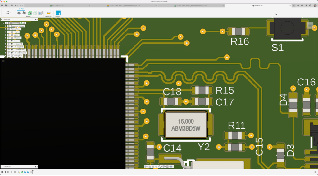
While designing a PCB with USB 3.0, it might get challenging to decide the spacing between traces that don’t allow interference or crosstalk. For this reason, PCB designers use the 5W rules, which means the distance between two traces must be equal to five times the width of the trace. You might increase the width for better performance. For instance, if a trace width is six mils, the gap between this trace and the next should be at least 30 mils.
In addition, you should keep a spacing of 30 mils from other signal traces. You can increase the distance to 50 mils if a high-speed trace is near a clock or a periodic signal because these might introduce larger crosstalk.
Avoiding crosstalk between high-speed interfaces in devices is essential. Before connector termination and after package escape, ensure no differential pair is routed within 30 mils of another differential pair to prevent crosstalk.
Rules for Additional High-Speed Differential Signals

- Avoid using test points or probes on high-speed differential signals.
- Avoid running high-speed traces through or close to magnetic components, ICs that use or generate clock signals, mounting holes, oscillators, clock signal generators, switching power regulators, or crystals.
- After BGA breakout, avoid exposing the SoC to high-speed differential signals since it may be challenging to filter out high current transients caused by internal state changes.
- When a GND layer is nearby, send high-speed differential pair signals to the top or bottom layers of the PCB. TI does not advise the high-speed differential signal strip-line routing.
- Be sure to route high-speed differential signals at least 90mils from the reference plane’s edge.
- Make sure high-speed differential signals are directed at least 1.5 W (estimated trace-width 1.5) away from holes in the reference plane. This requirement does not cover SMD pads on high-speed differential signals that have been voided.
- Maintain a steady trace width following the SoC BGA escape to prevent transmission line impedance mismatches.
- When possible, increase differential pair-to-pair spacing.
Symmetry in the Differential Pairs
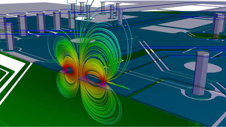
Another essential rule to remember is that differential pair traces must symmetrically and parallel to each other. You cannot route them if they have a component in between them. They must always be next to each other and routed in symmetry. However, this rule is violated when routing a connector pin or in case of packaging escape. In such cases, one must ensure the deviations are as short as possible.
Summary of PCB design
- The USB controller and the USB connector should be as close as possible to reduce the length of the trace.
- Ferrite beads and decoupling capacitors should be placed as close to the USB connector to decouple and eliminate high-frequency noise interference.
- Termination resistors should be placed as close to the USB controller as possible.
- The voltage regulator should also be placed as close to the connector.
Conclusion
When USB 3.0 was introduced in 2008, it quickly became one of the quickest means for transferring data. You might reach transfer rates of up to 5GB/s with the correct USB 3.0 cable, which is more than ten times what was previously achievable.
And if it still doesn’t meet your needs, you might want to look at the more recent and swifter successor standards, 3.1 and 3.2. In this manner, you can quickly back up your favorite images or charge your phone.
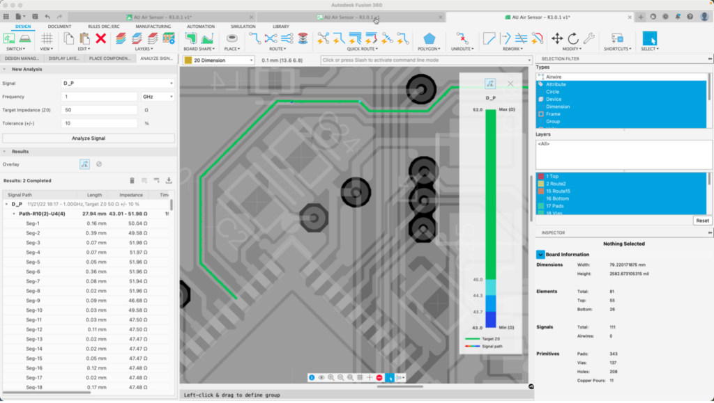
The Fusion 360 Signal Integrity Extension helps identify potential signal and power integrity issues and provides insight for optimizations to improve signal and power integrity performance. Lower your cost in prototypes and get to market sooner by obtaining the necessary details of your signal integrity traces by enabling the Fusion 360 electronic Signal Integrity extension powered by Ansys.